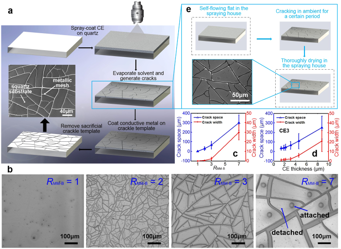
Figure 1. Fabrication process and optical and SEM characterizations of the CT-MM film.
(a) Schematic illustration of the fabrication steps for a large-area CT-MM film. The SEM image shows the highly connected metallic networks. (b) Optical images of crackle templates with different values of RMM-B, showing that the crack width and cell size can be controlled by the amount of monomers. (c) Experimental curves of crack width and crack spacing of the dried CEs with different values of RMM-B. (d) Variations in crack width and crack spacing with respect to coating thickness. (e) Drying process of crackle template. Inset: SEM image showing the fine cracks with ignorable buckling.

