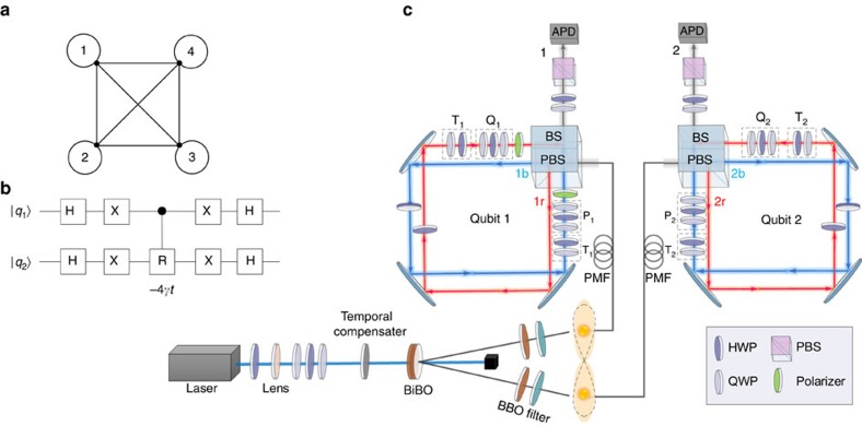
Figure 2. The schematic diagram and set-up of experimental demonstration.
(a) The K4 graph. (b) The quantum circuit for implementing CTQW on the K4 graph. This can also be used to implement CTQW on the K4 graph without self-loops, up to a global phase factor  . H and X represent the Hadamard and Pauli-X gate, respectively.
  is a phase gate. (c) The experimental set-up for a reconfigurable two-qubit photonics quantum processor, consisting of a polarization-entangled photon source using paired type-I BiBO crystal in the sandwich configuration and displaced Sagnac interferometers. See further details in Methods.

