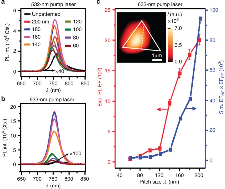
Figure 4. Photoluminescence of WSe2 on patterned gold nanostructures with different pitch sizes.
(a) 532-nm pump laser. (b) 633-nm pump laser. (c) Experimental PL enhancement factor (EF) (left axis) excited by 633-nm laser (after correcting for the trench area fraction) and the simulated EFNF (at 633 nm) × EFPF (at 750 nm) (right axis), respectively. The data points and corresponding error bars are obtained, respectively, by calculating the mean value and s.d. of PL EF based on 10 experimental PL spectra for each nanostructure. The inset shows the PL mapping of a WSe2 monolayer flake sited on patterned gold nanostructure with a pitch of 200 nm (on the left of the dashed line) and unpatterned gold film (on the right of the dashed line). The intensity value at each pixel was obtained by integrating the PL spectrum across the spectrum window of 700–820 nm. The solid line represent the shape of the flake and the dashed line represents the boundary between the patterned and unpatterned substrate. The laser power was 30 μW and integration time was 0.5 s.

