Abstract
We present a novel cost-efficient method for the fabrication of high-quality self-aligned plasmonic nanopores by means of optically controlled dielectric breakdown. Excitation of a plasmonic bowtie nanoantenna on a dielectric membrane localizes the high-voltage-driven breakdown of the membrane to the hotspot of the enhanced optical field, creating a nanopore that is automatically self-aligned to the plasmonic hotspot of the bowtie. We show that the approach provides precise control over the nanopore size and that these plasmonic nanopores can be used as single molecule DNA sensors with a performance matching that of TEM-drilled nanopores. The principle of optically controlled breakdown can also be used to fabricate non-plasmonic nanopores at a controlled position. Our novel fabrication process guarantees alignment of the nanopore with the optical hotspot of the nanoantenna, thus ensuring that pore-translocating biomolecules interact with the concentrated optical field that can be used for detection and manipulation of analytes.
Keywords: plasmonic nanopores, nanoplasmonics, solid-state nanopores, dielectric breakdown, DNA translocation
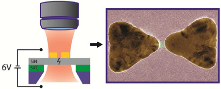
Graphical Abstract
Solid-state nanopores1–3 are biologically inspired sensors for label-free detection of single-biomolecules that show great promise for a large variety of applications, such as the investigation of proteins4,5, DNA-protein interactions6–8, protein-receptor binding9, and DNA sequencing.10,11 The elegance of nanopore biosensing relies in its robustness, versatility and simple working principle: the passage of biomolecules through a nanopore sensor modulates the nanopore ionic conductance, which serves as a means for detection and investigation of the target analyte.12,13 Yet, solid-state nanopores face challenges. For example, control over the translocation speed of the biomolecule14–17 is crucial for base-pair recognition on a DNA polymer, as already demonstrated using biological nanopores.18,19 Furthermore, it would be advantageous to expand the nanopore approach with new measuring modalities (e.g. optical detection) beyond mere electrical probing.
Recently, plasmonic solid-state nanopores were introduced,20–24 which present new opportunities for biomolecular sensing. Here, a plasmonic nanoantenna enhances and focuses electromagnetic radiation to a nanoscale volume (hotspot) right at the nanopore through which biomolecules can be translocated. Reports on plasmonic nanopores have so far mostly focused on nanoplasmonic heating.25–27 However, great promise lies in also exploiting the capabilities of these plasmonic nanostructures for extreme light-concentration to local nm-sized hotspots. Indeed, first examples of plasmon-enhanced optical detection of translocating analytes are already at hand.22,24 For these applications it is of paramount importance that the nanopore is precisely aligned with the optical hotspot to ensure that biomolecules pass the region of highest field localization.
Fabrication of plasmonic nanopores thus requires accurate positioning of the nanopore with respect to the plasmonic hotspot. Currently this is achieved by means of transmission electron microscopy (TEM) drilling or ion milling, where a beam of highly energetic charged particles locally ablates the membrane material to form a nanosized aperture.28–31 While providing nanometer-precise control of the nanopore size and shape,29 these drilling techniques have significant drawbacks: they are labor-intensive and not scalable, as fabrication is sequential and the constant presence of a machine operator is required. These issues make milling approaches for nanopore fabrication expensive and low-throughput. Recently however, an alternative method of in situ nanopore fabrication was introduced, based on the effect of dielectric breakdown.32,33 In this technique, a nanopore is rapidly formed upon local failure in the dielectric membrane, induced by applying a high transmembrane voltage that creates a large electric field (on the order of MV/cm) in the membrane.34 The size of the nanopore can be determined by monitoring the ionic transmembrane current that flows through the newly formed pore. Once the nanopore has reached a certain size, a lowering of the applied voltage can stop the breakdown process. Subsequently, the nanopore can be enlarged to any desired diameter by applying short voltage pulses,35 While the simple and inexpensive method of dielectric breakdown can provide high-quality nanopores,32,33 its use has so far been limited to applications that do not require control of the nanopore position.
Here, we demonstrate a method for self-aligned fabrication of plasmonic nanopores based on the promotion and localization of the dielectric breakdown by plasmonic excitation. By simultaneously electrically biasing the freestanding silicon-nitride membrane close to its critical field and applying laser excitation of a gold bowtie plasmonic nanostructure, we are able to induce the formation of a nanopore in the optical field hotspot of the bowtie nanoantenna. These fabricated plasmonic nanopores show a performance that is competitive with TEM-fabricated plasmonic nanopores,20,27 as demonstrated by optical beam profiling and detection of DNA translocations through the pores. The approach is cost-efficient, high-throughput and ensures that the nanopore is formed right in the gap of the bowtie antenna, which is essential for future applications of plasmonic nanopores for label-free biomolecule manipulation.
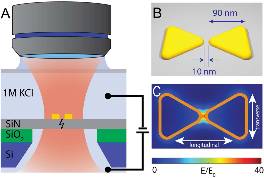
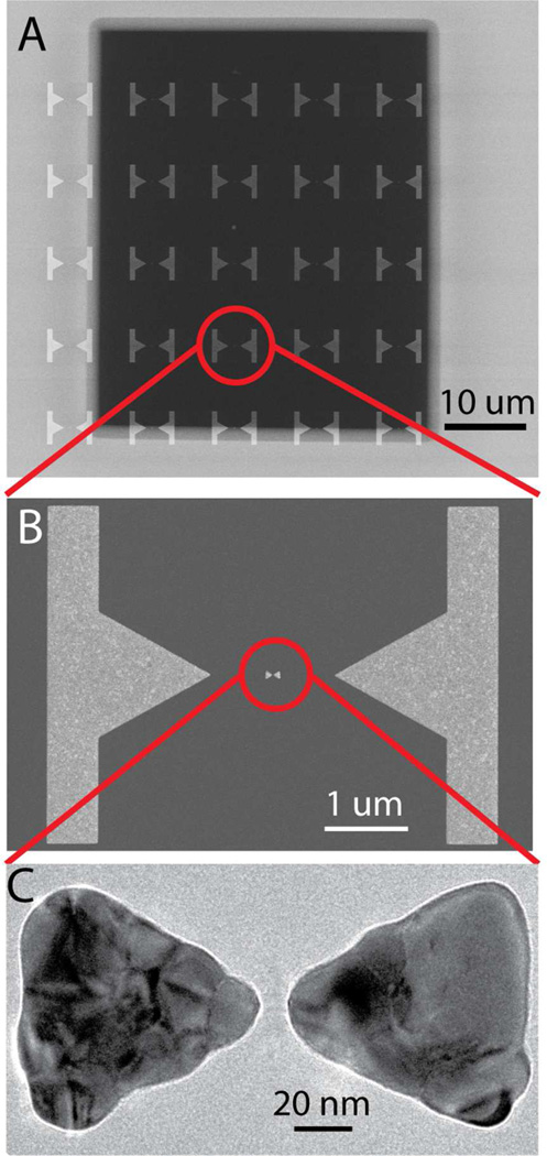
Figure 1A shows the concept of the plasmonic nanopore formation process, where a gold plasmonic bowtie antenna on a 20 nm thick low-stress silicon nitride-membrane is illuminated with a focused laser beam while a large transmembrane bias is applied. The gold bowtie nanoantenna (Figure 1B) consists of two 30 nm thick gold equilateral triangles of 90 nm size (tip-to-base) that face each other tip-to-tip with a 10 nm separation gap, fabricated using lift-off (see Methods for fabrication details). Figure 1C shows the results of a finite-difference time domain (FDTD) simulation for the optical field distribution around the bowtie at 785 nm incident wavelength. The structures can be illuminated at different polarizations of the laser beam, as indicated on Figure 1C: one along the main axis of the structures, termed the longitudinal mode of excitation, and one perpendicular to this axis, termed the transverse mode. For a longitudinal polarization of the incident light (Figure 1C), the optical field is clearly localized to the center of the bowtie structure (see SI for details). The hotspot of the evanescent field between the gold structures produces field enhancements up to 40 times compared to the incident field strength at the illumination wavelength. We used large metal markers to align the plasmonic nanostructure with our focused 785 nm wavelength laser. Figure 2A shows a scanning electron microscopy (SEM) image of a freestanding silicon nitride membrane with these metal markers. The separation between the metal markers and the plasmonic bowtie antenna is more than 500 nm (see Figure 2B), to prevent optical coupling of the nanoantenna to the metal markers. Figure 2C shows a transmission electron microscopy (TEM) image of the nanostructure. The triangles have slightly rounded tips resulting from the fabrication process, which was accounted for in the optical field simulations (Figure 1C).
Figure 1.
(A) Side-view sketch of the experimental layout. The membrane is exposed to a DC electric field and to the optical field that is locally enhanced by the plasmonic antenna. (B) Sketch of the plasmonic bowtie antenna on top of the freestanding silicon-nitride membrane. Typical sizes are indicated. (C) Result of a simulation of the electric field distribution (E) compared to the incident electric field amplitude (E0) at longitudinal excitation at a wavelength of 785 nm. Orange frames outline the position of the plasmonic structures in the model. The different polarization directions (longitudinal and transverse) of the excitation light is indicated with an arrow.
Figure 2.
(A) SEM image of a freestanding silicon-nitride membrane and gold marker structures. (B) SEM image of the gold plasmonic nanostructure (in the center) and two gold markers used to optically align the laser focus with the nanostructures. (C) Close-up TEM image of a plasmonic bowtie antenna on the membrane (without a pore yet).
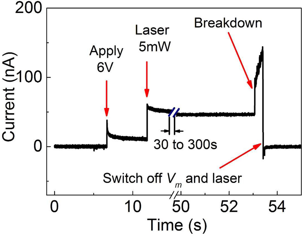
Fabrication of a nanopore using plasmonic dielectric breakdown starts with assembling the sample in an optically accessible flow cell as described in Ref. 36 and flushing in 1 M KCl or 2 M LiCl electrolyte solution. The electrolyte solution was buffered to pH 8 with 10 mM Tris-Cl and 1 mM EDTA to provide better control over the breakdown process.33 After aligning the diffraction-limited laser spot (~0.5 μm in size) with the plasmonic nanostructure, the membrane bias voltage is applied using Ag/AgCl electrodes (see Methods for experimental details). Figure 3 shows an example time-trace of the current through the membrane during a breakdown experiment. First, applying a transmembrane voltage of Vm = 6V results in a leakage current due to trap-assisted tunneling.37 No pore formation occurs with these settings, even after long times, as discussed in more detail below. Next, we keep the applied voltage and add illumination of the selected plasmonic bowtie structure with 5 mW laser power in longitudinal mode. This often increases the leakage current (see Figure 3), although quantitatively this varies from sample to sample. Then, within the next 30 s to 300 s, we suddenly discern a very rapid increase of the current across the membrane. This signifies the plasmonic dielectric breakdown event, which is associated with the formation of a nanopore (Figure 3). After reaching a certain preset threshold (130 nA in this case), both the bias voltage and the laser illumination are switched off to allow further control over the size of the nanopore. The resulting nanopores have a 70 to 130 MΩ resistance, corresponding to a nanopore diameter smaller than 4.5 nm using the model of Kowalczyk et al. for the nanopore conduction with the effective pore length taken as 8.6 nm.38 Such a small pore can be further enlarged to any desired diameter by subsequent applying moderate voltage pulses.35 After sizing the breakdown pore to the desired diameter, it is left overnight in 4M LiCl solution to equilibrate as in Ref. 32 before DNA translocation experiment. Equilibration is thought to occur as the nanopore surface slowly rearranges over time into a energetically more favorable shape.28
Figure 3.
Time trace of the transmembrane current during the formation of a plasmonic solid-state nanopore by dielectric breakdown.
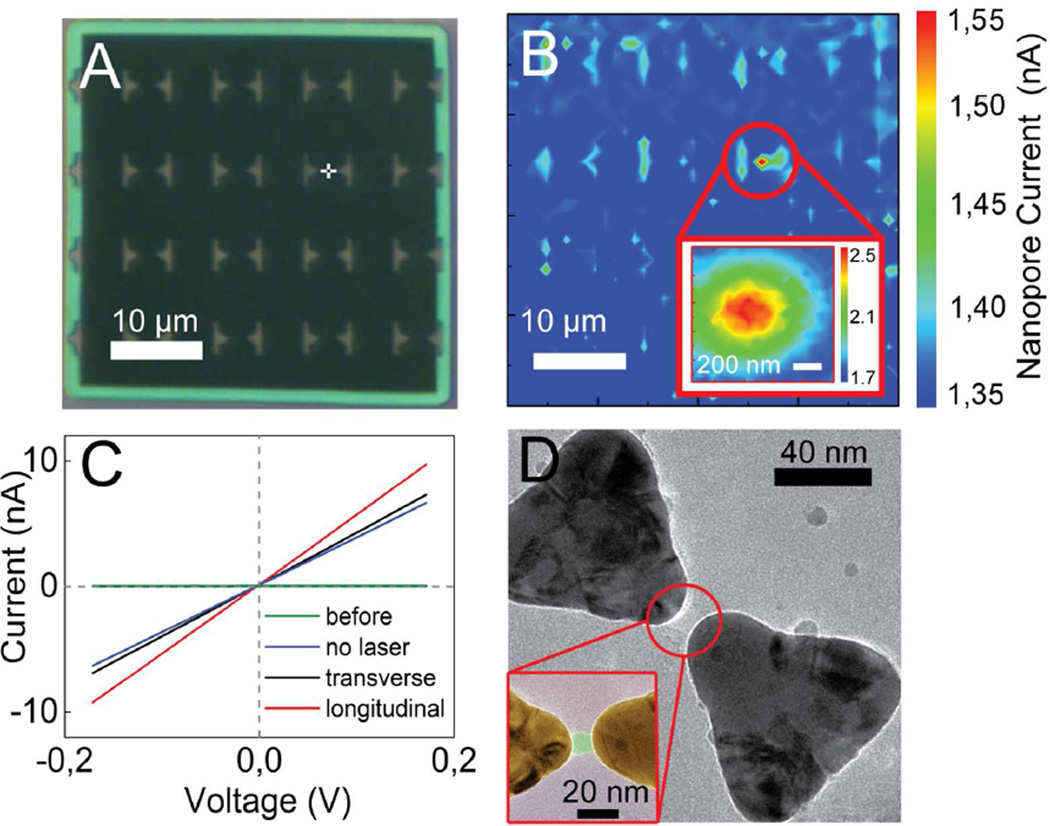
We are able to locate the nanopore in the plasmonic nanopore setup directly after its formation and enlargement. Figure 4A shows the freestanding silicon nitride membrane where the white cross indicates the point where we intended to create a plasmonic nanopore by illuminating a bowtie that was located at that position. After the breakdown, the pore location was determined by scanning the membrane with a low-power (0.5 mW) laser beam and simultaneous monitoring of the nanopore current at 100 mV transmembrane voltage (Figure 4B). When the laser focus illuminates the plasmonic nanostructure in the vicinity of the fabricated nanopore, localized heating of the plasmonic structure causes a local increase of the electrolyte conductivity27, and hence an increase in the ionic current through the pore, which results in an absolute maximum on the current map. The location of the maximum in Figure 4B confirms that the nanopore was indeed successfully formed at the position of the plasmonic bowtie that was illuminated with the laser during pore formation (Figure 4A). The inset of Figure 4B shows a higher-resolution membrane scan of the area in the vicinity of the nanopore. To characterize the located nanopore we measure the I-V curves of the formed pore under transverse and longitudinal laser polarizations, as shown in Figure 4C. Linear I-V curves are observed. The creation of the pore drastically changed the resistance from >1GΩ before breakdown to a value of 26.6 MΩ. Upon laser illumination, the pore resistance changes to 24.3 MΩ and 18.1 MΩ for transverse and longitudinal excitation respectively, which indicates that the fabricated pore is in close proximity to a plasmonic nanostructure and that the absorption cross-section of the bowtie nanoantenna in longitudinal mode is higher than in transverse mode.
Figure 4.
(A) Optical image of the freestanding silicon-nitride membrane with gold markers indicating the positions of the plasmonic nanostructures. The position of the laser spot that is used to induce the formation of the nanopore, and hence the desired nanopore location, are indicated by a white cross. (B) Ionic current map of the membrane at 100 mV bias at low (0.5 mW) laser power after pore formation. The inset is a higher resolution scan of the area near the nanopore. (C) Current-voltage characteristics of the fabricated pore acquired with and without laser excitation of the plasmonic bowtie antenna. Green line corresponds to the current-voltage characteristic of the freestanding membrane before breakdown event. (D) Typical TEM image of a nanopore fabricated using plasmonic dielectric breakdown. The zoom in the inset shows a false-colored image of the gap of the gold bowtie structure that more clearly visualizes the nanopore.
TEM microscopy allowed for a careful visualization of the nanopore. Figure 4D shows a typical TEM image of a plasmonic nanopore that was fabricated by means of plasmonic dielectric breakdown in longitudinal mode. In agreement with our hypothesis, the nanopore has formed right in the gap of the bowtie structure, where the hotspots of the optical field are located (clear from the false-colored inset in Figure 4D). Whereas a temperature elevation is known to promote dielectric breakdown,39 this would cause the pore to form anywhere around the nanostructure, as the temperature profile over the ~100nm nanostructure is nearly uniform.40 Instead, we observe that pores form consistently at the center of the bowtie (see additional examples in SI), confirming that the plasmonic optical field enhancement plays an essential role in the localization of the breakdown effect.
In order to set proper conditions for plasmonic dielectric breakdown we selected an applied voltage of Vm = 6 V. This was the highest attainable voltage that was insufficient to generate a dielectric breakdown in absence of plasmonic excitation, within at least 30 min of observation. Such a Vm creates an electric field strength of 3 MV/cm in the 20 nm thick dielectric membrane, which is at least 3 times lower than the breakdown field of low-stress silicon-nitride films as reported in the literature.41,42 Staying below the breakdown field safeguards us against the occurrence of a regular breakdown event,33 which would result in the formation of a nanopore in a random location on the membrane. Notably, the optical field in the hotspot of the bowtie antenna at 5 mW of laser power is estimated to produce an optical field of 1.5 MV/cm in the plasmonic hotspot (See SI for details) that is spatially localized to a small volume of a few nanometers. While providing an additional electromagnetic field at the position for pore formation, this highly nonuniform optical field has a different nature than the applied DC electric field.
A number of control experiments confirm that the plasmonic dielectric breakdown is the result of synergetic influence of the DC electric field and the plasmonic optical field on the membrane. First, we verified that the pores made by regular dielectric breakdown, without laser illumination, at Vm higher than 7 V did indeed form in a random location on the freestanding membrane, unaffected by the presence of the plasmonic nanostructures. Using higher laser powers, the pore can be located by scanning the membrane as described above (See SI for the details). Second, we demonstrate that, interesting in itself, the optical field of the laser is capable of localizing the breakdown event also without plasmonic structures, provided that a much higher laser power (45 mW) is used (See SI). This confirms that it is the optical nature of the excitation that promotes the dielectric breakdown rather than mere temperature elevation. In passing, we note that this also provides a novel means to control the position of nonplasmonic nanopores using dielectric breakdown.
To demonstrate that plasmonic nanopores drilled by controlled dielectric breakdown can be used as high-quality single molecule biosensors, we performed DNA translocation experiments on such nanopores with and without laser excitation of the plasmonic nanostructures. Under application of a bias voltage across the membrane, DNA molecules are electrophoretically attracted to the nanopore and then driven through it, thus leading to a transient reduction of the ionic current, as the passing molecule obstructs part of the ion flow through the nanopore.
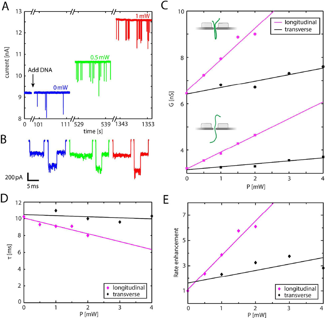
Figure 5A shows 3 typical time traces of the current at 100 mV during a DNA translocation experiment through a 11.0 MΩ nanopore, equivalent to an effective diameter of 10.6 nm in 2 M LiCl at 0 mW, 0.5 mW, and 1 mW of excitation power in longitudinal mode (see SI for details). After the addition of 5 ng/μL λ-DNA (48.5 kbp), transient current blockades can clearly be observed for all 3 illumination conditions. Figure 5B shows zooms of 6 DNA translocation events in a linear (left) and folded fashion (right). The clear distinct conductance levels reflect that the fabricated plasmonic nanopore exhibits excellent signal-to-noise characteristics, at least on-par with nanopores drilled using TEM (see SI).20,43 Figure 5C displays the conductance blockade levels ΔG change with laser power in longitudinal and transverse excitation. The blockade levels rise linearly with increasing laser power, in quantitative agreement with data for the TEM-drilled plasmonic nanopores20, which can be explained by plasmonic heating. Figure 5D shows the translocation times of the DNA molecules. While, based on a locally heated nanopore, no significant dependence on the laser power is expected,20 the translocation times decrease slightly with laser power for longitudinal polarization, but not for transverse polarization. Finally, Figure 5E shows a strong enhancement of the rate at which the DNA molecules are captured into the nanopore with increasing of the laser power, where the longitudinal mode shows a stronger enhancement than the transverse mode of excitation. This rate enhancement in LiCl is in good agreement with the results obtained in TEM drilled plasmonic nanopores and can be explained by plasmon-induced thermophoretic capture of DNA.20
Figure 5.
(A) Time trace of the ionic current through a dielectric–breakdown-fabricated plasmonic nanopore, during DNA translocations under 100 mV bias voltage at 0 mW (blue), 0.5 mW (green) and 1 mW (red) plasmonic excitation in longitudinal polarization. (B) Sample events for a linear translocation and a folded translocation at 0 mW (blue), 0.5 mW (green) and 1 mW (red) low-pass filtered at 10 kHz. (C) Conductance blockade levels ΔG, for the single blockade-level (squares, one double strand of DNA inside the nanopore) and the double blockade level (circles, two double strands of DNA inside the nanopore) as a function of illumination power for longitudinal (magenta) and transverse (black) polarization. The full lines are linear fits. (D) DNA translocation times τ as a function of illumination power for longitudinal (magenta) and transverse (black) polarization. Lines are linear fits. (E) Event rate enhancement versus laser power for both longitudinal (magenta) and transverse excitation (black). Lines are linear fits. Standard errors of the mean were in all cases smaller than the marker symbols and hence error bars are omitted in the plots.
In summary, we have developed a novel method for self-aligned formation of nanopores in plasmonic hotspots by means of controlled dielectric breakdown. The breakdown event is initiated at the optical field hotspot of the plasmonic nanostructure by applying a large DC electric field applied across a thin membrane while simultaneous optically illuminating the plasmonic nanostructure on the membrane. This ensures that the nanopore is automatically positioned at the location of highest field intensity. Interestingly, this makes the method particularly suitable also for plasmonic systems where the position of the most intense hot spot is not previously known or difficult to predict.44 We have demonstrated DNA translocations through these nanopores and have shown that they perform on-par with TEM-drilled plasmonic nanopores in both their noise and DNA-translocation characteristics. The method presented is cost-efficient and high-throughput. Since the approach results in a nanopore that is automatically aligned with the optical hotspot of the plasmonic nanostructure, the method is perfectly suited for high-yield fabrication of plasmonic nanopores, promising for applications such as fluorescence detection, Raman characterization, DNA sequencing, and trapping of single biomolecules.
Methods
Sample Fabrication
Chips with 30×30 μm 20 nm thick free-standing silicon-nitride membranes were fabricated as described in Ref. 45, where transmembrane patterning was omitted to expose the full silicon-nitride surface. Plasmonic nanostructures and alignment marker structures were fabricated on top of the free-standing membranes using e-beam lithography patterning of a single-layer PMMA 950K resist. After development, an adhesion layer of 1 nm Ti was evaporated on the sample followed by evaporation of 30 nm of gold. Then the PMMA layer was subsequently removed using lift-off.
Alignment of laser focus with plasmonic structure before breakdown
The position of the laser focus was aligned to the plasmonic nanostructure using the large metal markers and a piezoelectric positioning stage (PI GmbH), while being imaged using a 60x 1.2 NA water-immersion objective (Olympus). The same objective was used to focus the 785 nm wavelength laser to a diffraction-limited laser spot size of about 0.5 μm, which was enough for sufficiently accurate alignment of the laser focus and the plasmonic nanostructure using the markers. The plasmonic nanostructures were not exposed to laser illumination during the alignment procedure.
Electronic Instrumentation
For plasmonic dielectric breakdown, we used a custom-build current amplifier, capable of applying ±20 V and recording sub-nA currents, as described in more detail in Ref. 33. I-V and ionic current measurements during nanopore localization and DNA translocations are recorded using a commercial amplifier, Axopatch 200B (Molecular Devices, LLC) with a four-pole Bessel filter set at 100 kHz.
FDTD Simulations
We used FDTD Solutions (Lumerical Solutions, Inc., Canada) to model the optical properties of the plasmonic bowtie nanoantenna. The bowtie antenna was modeled as two 30 nm thick gold equilateral triangles of 90 nm in size (tip-to-base) that face each other tip-to-tip with a 10 nm separation. The corners of the triangles were rounded (15 nm-in-radius rounding) to better resemble the fabricated structures. The antenna was positioned on a 20 nm thin silicon-nitride membrane with a refractive index (RI) of 2 and 1 nm native oxide layer of RI = 1.4. The surrounding medium was modeled as water with a RI of 1.33. Symmetry was used to reduce the computational time. The plasmonic antenna was excited by a pulse from a total-field scattered-field source incident normal to the membrane, and with the polarization in either the longitudinal or the transverse mode. The optical absorption cross section was calculated by the net power flux through a box surrounding the antenna.
Supplementary Material
Acknowledgments
We would like to acknowledge Aleksei Aksimentiev for valuable discussions. This work was supported by the National Human Genome Research Institute of the National Institute of Health under Award Number 1R01HG007406-01, by a Wenner-Gren Fellowship from the Wenner-Gren Foundations, by ERC Advanced grants NanoforBio (no. 247072) and SynDiv (no. 669598) and by the Netherlands Organisation for Scientific Research (NWO/OCW), as part of the Frontiers of Nanoscience program.
Footnotes
Associated Content
Supporting Information. Additional TEM images of plasmonic nanopores fabricated using plasmonic dielectric breakdown, results on laser-promoted (non-plasmonic) dielectric breakdown, localization of regular dielectric breakdown (no laser), results on FDTD simulations of field enhancements and absorption cross-sections of bowtie nanoantennas, estimation of optical field strength in plasmonic hotspot, noise spectra of plasmonic nanopores, results on plasmonic nanopore conductance versus diameter, discussion on diameter determination of plasmonic nanopore used for DNA translocations, and results on the relative current increase versus laser power. This material is available free of charge via the Internet at http://pubs.acs.org.
Author Contributions
The manuscript was written through contributions of all authors. All authors have given approval to the final version of the manuscript.
References
- 1.Dekker C. Nat. Nanotechnol. 2007;2(4):209–215. doi: 10.1038/nnano.2007.27. [DOI] [PubMed] [Google Scholar]
- 2.Wanunu M. Phys. Life Rev. 2012;9(2):125–158. doi: 10.1016/j.plrev.2012.05.010. [DOI] [PMC free article] [PubMed] [Google Scholar]
- 3.Muthukumar M, Plesa C, Dekker C. Phys. Today. 2015;68(8):40–46. [Google Scholar]
- 4.Bonome EL, Lepore R, Raimondo D, Cecconi F, Tramontano A, Chinappi M. J. Phys. Chem. B. 2015;119(18):5815–5823. doi: 10.1021/acs.jpcb.5b02172. [DOI] [PubMed] [Google Scholar]
- 5.Cressiot B, Oukhaled A, Bacri L, Pelta J. Bionanoscience. 2014;4(2):111–118. [Google Scholar]
- 6.Japrung D, Bahrami A, Nadzeyka A, Peto L, Bauerdick S, Edel JB, Albrecht T. J. Phys. Chem. B. 2014;118:11605–11612. doi: 10.1021/jp506832u. [DOI] [PubMed] [Google Scholar]
- 7.Marshall MM, Ruzicka Ja, Zahid OK, Henrich VC, Hall AR, Taylor EW. Langmuir. 2015:150403172344006. doi: 10.1021/acs.langmuir.5b00457. [DOI] [PubMed] [Google Scholar]
- 8.Plesa C, Ruitenberg JW, Witteveen MJ, Dekker C. Nano Lett. 2015;15:3153–3158. doi: 10.1021/acs.nanolett.5b00249. [DOI] [PubMed] [Google Scholar]
- 9.Wei R, Gatterdam V, Wieneke R, Tampe R, Rant U. Nat. Nanotechnol. 2012;7(4):257–263. doi: 10.1038/nnano.2012.24. [DOI] [PubMed] [Google Scholar]
- 10.Ando G, Hyun C, Li J, Mitsui T. ACS Nano. 2012;6(11):10090–10097. doi: 10.1021/nn303816w. [DOI] [PMC free article] [PubMed] [Google Scholar]
- 11.Carlsen AT, Zahid OK, Ruzicka J, Taylor EW, Hall AR. ACS Nano. 2014;8(5):4754–4760. doi: 10.1021/nn501694n. [DOI] [PubMed] [Google Scholar]
- 12.Muthukumar M. Annu. Rev. Biophys. Biomol. Struct. 2007;36:435–450. doi: 10.1146/annurev.biophys.36.040306.132622. [DOI] [PubMed] [Google Scholar]
- 13.Chang H, Kosari F, Andreadakis G, Alam Ma, Vasmatzis G, Bashir R. Nano Lett. 2004;4(8):1551–1556. [Google Scholar]
- 14.Fologea D, Uplinger J, Thomas B, Mcnabb DS, Li J. Nano Lett. 2005;5(9):1734–1737. doi: 10.1021/nl051063o. [DOI] [PMC free article] [PubMed] [Google Scholar]
- 15.Smeets RMMMM, Keyser UF, Krapf D, Wu M-Y, Dekker NH, Dekker C. Nano Lett. 2006;6(1):89–95. doi: 10.1021/nl052107w. [DOI] [PubMed] [Google Scholar]
- 16.Keyser UFF. J. R. Soc. Interface. 2011;8(63):1369–1378. doi: 10.1098/rsif.2011.0222. [DOI] [PMC free article] [PubMed] [Google Scholar]
- 17.Plesa C, Loo NVan, Ketterer P, Dietz H, Dekker C. Nano Lett. 2015;15:732–737. doi: 10.1021/nl504375c. [DOI] [PubMed] [Google Scholar]
- 18.Clarke J, Wu H-C, Jayasinghe L, Patel A, Reid S, Bayley H. Nat. Nanotechnol. 2009;4(4):265–270. doi: 10.1038/nnano.2009.12. [DOI] [PubMed] [Google Scholar]
- 19.Manrao Ea, Derrington IM, Laszlo AH, Langford KW, Hopper MK, Gillgren N, Pavlenok M, Niederweis M, Gundlach JH. Nat. Biotechnol. 2012;30(4):349–353. doi: 10.1038/nbt.2171. [DOI] [PMC free article] [PubMed] [Google Scholar]
- 20.Nicoli F, Verschueren D, Klein M, Dekker C, Jonsson MP. Nano Lett. 2014;14(12):6917–6925. doi: 10.1021/nl503034j. [DOI] [PMC free article] [PubMed] [Google Scholar]
- 21.Belkin M, Chao S, Jonsson M, Dekker C, Aksimentiev A. Submitt. to ACS Nano. doi: 10.1021/acsnano.5b04173. [DOI] [PMC free article] [PubMed] [Google Scholar]
- 22.Cecchini MP, Wiener A, Turek VA, Chon H, Lee S, Ivanov AP, Mccomb DW, Choo J, Albrecht T, Maier SA, Edel JB. Nano Lett. 2013;13:4602–4609. doi: 10.1021/nl402108g. [DOI] [PubMed] [Google Scholar]
- 23.Chen C, Juan ML, Li Y, Maes G, Borghs G, Van Dorpe P, Quidant R. Nano Lett. 2012;12(1):125–132. doi: 10.1021/nl2031458. [DOI] [PubMed] [Google Scholar]
- 24.Nam S, Choi I, Fu C, Kim K, Hong S, Choi Y, Zettl A, Lee LP. Nano Lett. 2014;14:5584–5589. doi: 10.1021/nl503159d. [DOI] [PubMed] [Google Scholar]
- 25.Li Y, Nicoli F, Chen C, Lagae L, Groeseneken G, Stakenborg T, Zandbergen HW, Dekker C, Dorpe P Van, Jonsson MP. Nano Lett. 2015;15(1):776–782. doi: 10.1021/nl504516d. [DOI] [PMC free article] [PubMed] [Google Scholar]
- 26.Crick CR, Albella P, Ng B, Ivanov AP, Roschuk T, Cecchini MP, Bresme F, Maier SA, Edel JB. Nano Lett. 2015;15:553–559. doi: 10.1021/nl504536j. [DOI] [PubMed] [Google Scholar]
- 27.Jonsson MPP, Dekker C. Nano Lett. 2013;13(3):1029–1033. doi: 10.1021/nl304213s. [DOI] [PubMed] [Google Scholar]
- 28.Van den Hout M, Hall AR, Wu MY, Zandbergen HW, Dekker C, Dekker NH. Nanotechnology. 2010;21(11):115304. doi: 10.1088/0957-4484/21/11/115304. [DOI] [PubMed] [Google Scholar]
- 29.Storm AJ, Chen JH, Ling XS, Zandbergen HW, Dekker C. Nat. Mater. 2003;2(8):537–540. doi: 10.1038/nmat941. [DOI] [PubMed] [Google Scholar]
- 30.Ahmadi AG, Peng Z, Hesketh PJ, Nair S. J. Micro/Nanolithography, MEMS MOEMS. 2010;9(3):033011. [Google Scholar]
- 31.Lanyon YH, De Marzi G, Watson YE, Quinn AJ, Gleeson JP, Redmond G, Arrigan DWM. Anal. Chem. 2007;79(8):3048–3055. doi: 10.1021/ac061878x. [DOI] [PubMed] [Google Scholar]
- 32.Briggs K, Kwok H, Tabard-Cossa V. Small. 2014;10(10):2077–2086. doi: 10.1002/smll.201303602. [DOI] [PubMed] [Google Scholar]
- 33.Kwok H, Briggs K, Tabard-Cossa V. PLoS One. 2014;9(3) doi: 10.1371/journal.pone.0092880. [DOI] [PMC free article] [PubMed] [Google Scholar]
- 34.Sze SM. J. Appl. Phys. 1967;38(7):2951–2956. [Google Scholar]
- 35.Beamish E, Kwok H, Tabard-Cossa V, Godin M. Nanotechnology. 2012;23(40):405301. doi: 10.1088/0957-4484/23/40/405301. [DOI] [PubMed] [Google Scholar]
- 36.Van Dorp S, Keyser UF, Dekker NH, Dekker C, Lemay SG. Nat. Phys. 2009;5(5):347–351. [Google Scholar]
- 37.Briggs K, Charron M, Kwok H, Le T, Chahal S, Bustamante J, Waugh M, Tabard-Cossa V. Nanotechnology. 2015;26(8):084004. doi: 10.1088/0957-4484/26/8/084004. [DOI] [PubMed] [Google Scholar]
- 38.Kowalczyk SW, Grosberg AY, Rabin Y, Dekker C. Nanotechnology. 2011;22(31):315101. doi: 10.1088/0957-4484/22/31/315101. [DOI] [PubMed] [Google Scholar]
- 39.Kimura M. IEEE Trans. Electron Devices. 1999;46(1):220–229. [Google Scholar]
- 40.Baffou G, Quidant R. Laser Photonics Rev. 2013;7(2):171–187. [Google Scholar]
- 41.Habermehl S, Apodaca RT, Kaplar RJ. Appl. Phys. Lett. 2009;94(1):10–13. [Google Scholar]
- 42.Lombardo S, Stathis JH, Linder BP, Pey KL, Palumbo F, Tung CH. J. Appl. Phys. 2005;98(12) [Google Scholar]
- 43.Kowalczyk SW, Wells DB, Aksimentiev A, Dekker C. Nano Lett. 2012;12:1038–1044. doi: 10.1021/nl204273h. [DOI] [PMC free article] [PubMed] [Google Scholar]
- 44.Langer J, Novikov SM, Liz-Marzan LM. Nanotechnology. 2015;26(32):322001. doi: 10.1088/0957-4484/26/32/322001. [DOI] [PubMed] [Google Scholar]
- 45.Janssen XJa, Jonsson MP, Plesa C, Soni GV, Dekker C, Dekker NH. Nanotechnology. 2012;23(47):475302. doi: 10.1088/0957-4484/23/47/475302. [DOI] [PubMed] [Google Scholar]
Associated Data
This section collects any data citations, data availability statements, or supplementary materials included in this article.


