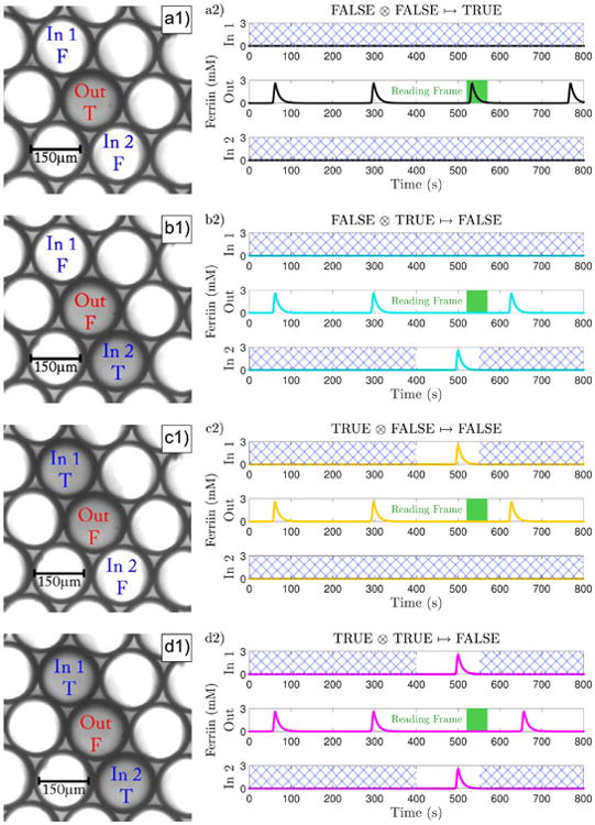
Fig. 2.

NOR gate droplet configuration and timing diagram. (a, b, c, d) Correspond to the four possible logic states of the inputs to a NOR gate; FF, TF, FT, TT. (a1, b1, c1, d1) Photographs of the BZ drops that comprise the NOR gate. (a2, b2, c2, d2) Timing diagrams of simulations of the NOR gate in which a high concentration of ferriin corresponds to the logic TRUE state, a low value to the logic FALSE state. The hatched area on the inputs represents the time during which light is applied to inhibit the droplets. The green box is the reading frame. (a) Both inputs are constantly suppressed with light and never spike; thus they are registered as FALSE. The output is unperturbed and spikes inside the reading frame; thus it is read as TRUE. (b-c) One input is constantly suppressed (FALSE) while light is removed from the second, allowing it to spike and hence is registered as TRUE. The output is perturbed and spikes outside the reading frame; thus it is read as FALSE. (d) Light is removed from both inputs allowing both to spike (TRUE). The output is perturbed and spikes outside the reading frame; thus it is read as FALSE.
