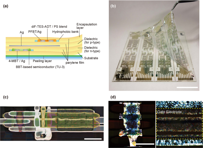
Figure 1. Ultrathin organic CMOS logic circuits using a stacked structure.
(a) Complete structure for the stacked devices. (b) Photograph of organic CMOS logic circuit on a one-micron (μ m) substrate. The total thickness was less than 3 μ m. Scale bar, 25 mm. (c) Image of the CMOS inverter constituting the D-FF circuit. Scale bar, 500 μ m. (d) Polarized microscope image of the diF-TES-ADT/PS blend and TU-3. Scale bar, 250 μ m.

