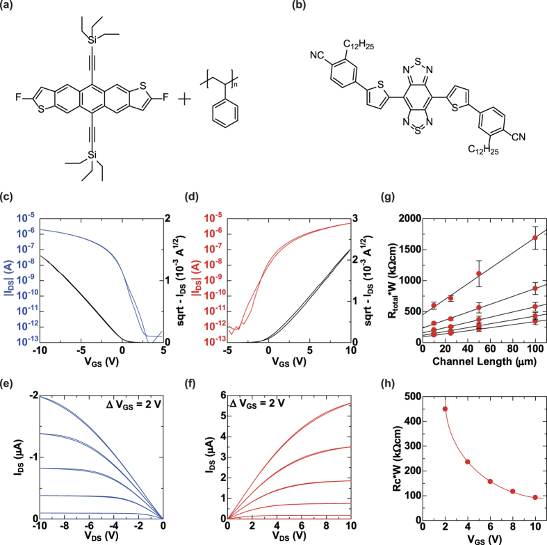
Figure 2. Molecular structure and transistor features of printed OTFTs.
Molecular structure of (a) the p-type semiconductor (diF-TES-ADT and PS) and (b) the n-type semiconductor (TU-3). Transfer characteristics of (c) the p-type OTFT with VDS = − 10 V and (d) the n-type OTFT with VDS = 10 V. Saturation mobilities are 0.34 and 0.21 cm2 V−1 sec−1, respectively. Output characteristics of the (e) p-type OTFT and (f) n-type OTFT. (g) Channel width-normalized total resistance (Rtotal) as a function of channel length. (h) Width-normalized contact resistance (Rc) as a function of VGS. The width-normalized contact resistance was 92.6 k Ω cm at VGS = 10 V.

