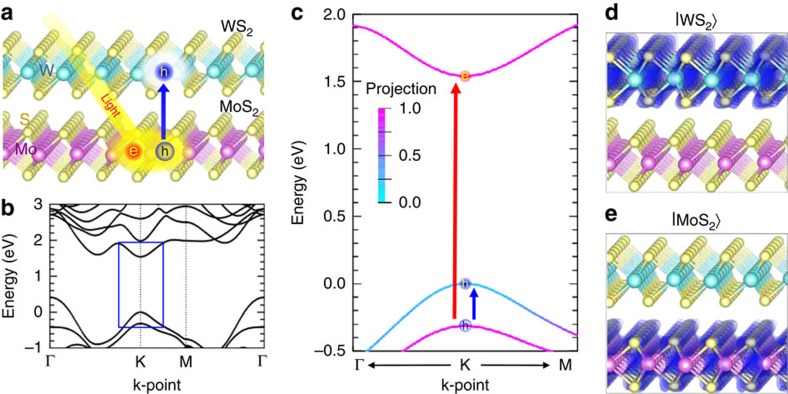
Figure 1. Atomic and electronic structures of MoS2/WS2 heterostructures.
(a) Illustration of the heterostructure, where a WS2 monolayer lies on top of a MoS2 monolayer. Electron and hole carriers excited by incident light separate by hole transfer into the WS2. (b) Band structure of the heterostructure, showing an indirect bandgap from Γ to K. The smallest direct transition with appreciable absorption is from the (VBM-1) state to the CBM in the vicinity of K. (c) Band structure in the vicinity of K-point in the Brillouin zone. From the K-point at the centre, right and left are directions toward Γ and M points, respectively. The incident light excites electron in |MoS2〉 to the conduction band minimum, and hole is transferred into |WS2〉. The energy of the valence band maximum at the K-point is set to zero. Colour indicates the degree of projection of each state onto the MoS2 layer. A projection of one (pink) indicates complete localization of the state to the MoS2 layer and that of zero (blue) indicates localization to the WS2 layer. (d,e) Isosurface plots of two valence band charge density at the K-point. The local VBM, which we denote |WS2〉, presents almost entirely localized charge to WS2 (d), but the (VBM-1) state, which we denote|MoS2〉, is almost entirely localized to MoS2 (e).

