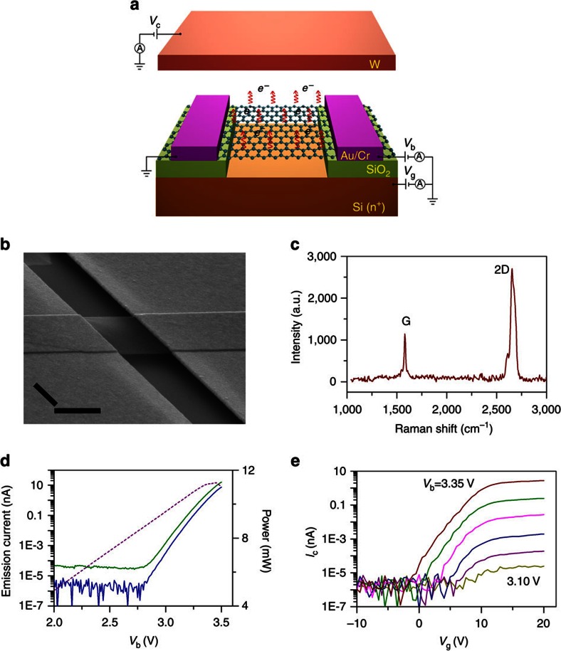
Figure 1. Structure and electron emission performances of a GME.
(a) A schematic drawing showing the structure of a GME and its working principle. A GME is fabricated on a SiO2/Si wafer substrate and consists of a graphene film suspended between two metal (Au/Cr) electrodes and over the bottom Si electrode. A bias voltage (Vb) is applied to a GME to drive the electron emission from it and a top W electrode with a collecting voltage (Vc) applied is used to collect and measure the emission current. The highly doped Si layer applied with a voltage of Vg acts as the gate to tune the emission current measured by the top W electrode. (b) Tilted SEM image of a GME (scale bar, 1 μm). (c) Raman spectrum of a GME exhibiting a G peak of 1,580 cm−1 and a 2D peak of 2,656 cm−1. (d) Emission current of a GME measured by the upper collector electrode (Ic, solid blue line) and the bottom gate electrode (Ig, solid olive line) and the corresponding applied Joule-heating power (dashed purple line) when ramping up Vb and fixing Vc (100 V) and Vg (15 V). (e) Ic−Vg curves of the same GME as in c when Vb increases from 3.10 to 3.35 V at 0.05 V intervals and Vc is fixed at 100 V.

