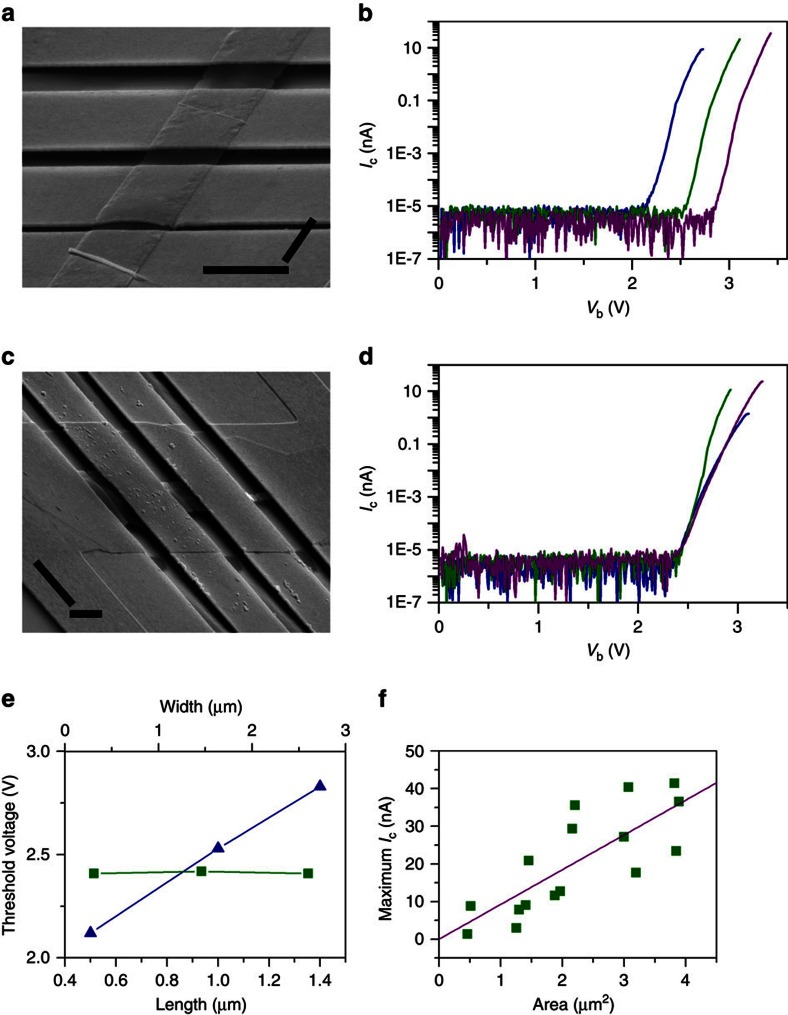
Figure 4. Electron emission performances of GMEs with different graphene dimensions.
(a) Tilted SEM image of three GMEs with the same width of 1.7 μm but different length of 0.5, 1.0 and 1.4 μm, respectively, after breakdown (scale bar, 2 μm). (b) Ic−Vb curves of the GMEs with the length of 0.5 μm (blue line), 1.0 μm (olive line) and 1.4 μm (purple line) as shown in a. (c) Tilted SEM image of three GMEs with the same length of 1.5 μm but different widths of 0.3, 1.5 and 2.6 μm, respectively, after breakdown (scale bar, 2 μm). (d) Ic–Vb curves of the GMEs with the width of 0.3 μm (blue line), 1.5 μm (olive line) and 2.6 μm (purple line) as shown in c. Ic−Vb curves in b and d were measured until the breakdown of GMEs due to excess electrical and thermal stress. (e) The plots of the turn-on threshold bias voltage versus the length (blue triangles) and width (olive squares) of the GMEs in b and d. (f) Maximum emission current (olive squares) of GMEs with different area. The solid line is the linear fitting of the data points. All data shown in this figure were measured at Vc=100 and Vg=10 V.

