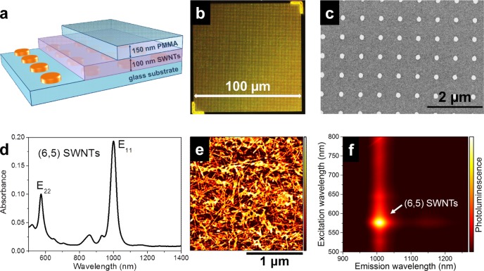
Figure 1.
(a) Schematic illustration of a sample consisting of a glass substrate, gold nanodisk array, a 100 nm layer of random (6,5) SWNTs and a 150 nm PMMA layer on top. (b) Dark-field microscopy image of nanodisk array under white-light illumination and (c) scanning electron micrograph of periodic array of gold nanodisks with 670 nm pitch (diameter 160–180 nm). (d) Representative absorption spectrum, (e) atomic-force micrograph, and (f) photoluminescence excitation map of a 100 nm thick (6,5) SWNT layer.

