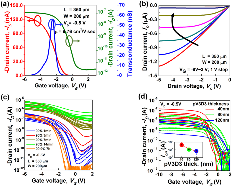
Figure 2.
(a) Transfer characteristics (green: log scale, red: linear scale) and gm vs. VG (blue) of the printed top-gate CNT-TFTs (L = 350 μm and W = 200 μm). (b) Output characteristics with various VG values ranging from −8 to 3 V. (c) Transfer characteristics with two semiconducting enriched nanotube solutions (90% and 99.9%) and various deposition times. (d) Transfer characteristics for several pV3D3 gate dielectric thicknesses (inset). The values of ION value were extracted from the transfer characteristics for each condition.

