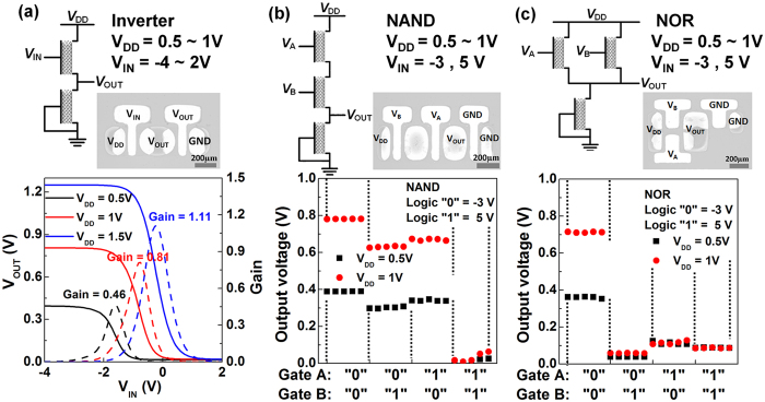
Figure 4. Inverter, 2-input NAND and NOR circuits using all p-type printed top-gate CNT-TFTs on a PES substrate with VDD 0.5 V, 1 V and 1.5 V.
(a) Schematic of the diode-load inverter using the CNT-TFTs with all p-type devices, an optical microscope image, and the inverter voltage transfer characteristic (solid lines) and the voltage gain (dashed lines). (b,c) Output voltages of the 2-input NAND and NOR circuit, respectively, where supply voltages VDD of 0.5 V and 1 V were applied. The input voltage of −3 V and 5 V are treated as logical “1” and “0”, respectively.

