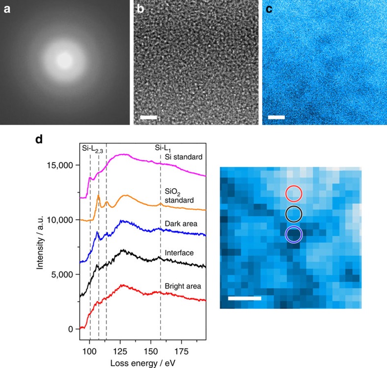
Figure 2. TEM/STEM micrographs and EELS spectra of amorphous SiO.
(a) Selected area electron diffraction pattern; (b) High-resolution TEM image; and (c) HAADF-STEM image of the amorphous SiO. Scale bar, 2 nm. (d) EELS profiles (Si-K edge) taken from the dark (blue circle), bright (red circle) and interfacial (black circle) regions in the HAADF-STEM image. Standard EELS profiles of amorphous Si and SiO2 were extracted from the literature11. Scale bar, 2 nm.

