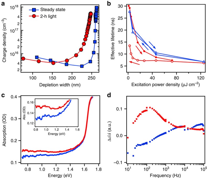
Figure 2. Evidence and characterization of light-activated meta-stable trap states.
(a) Charge density profile of the device steady state and after illumination for 2 h at an open-circuit condition. The right-hand side of the x-axis corresponds to the interface perovskite/contact layers, and the left-hand side locates the center of the active perovskite layer. (b) Light-excitation power density dependence of the effective PL lifetime of a thin film under continuous light soaking (red) and after recovery of the system in the dark between each data point (blue). Filled and open symbols represent excitation power density increase and decrease cycle, respectively. Lines between symbols are a guide to the eye. (c) Direct evidence into the deep-level trap states formed after white light soaking (red line) as compared with steady state thin (blue line) by near-infrared absorption measurement. The inset is zoomed-in region. (d) Low-frequency real dielectric constant relative change (Δɛ/ɛi) for a device illuminated for 2 h (red) and after recovery in dark (blue), as compared with steady state.

