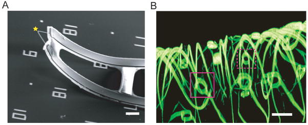
Figure 2. Flexible and three dimensional nanoelectronic devices.
(A) Scanning electron microscopy image of a single kinked nanowire probe used for intracellular potential recording. The yellow star highlights the position of a field effect transistor. Scale bar, 5 μm. (B) Confocal fluorescence microscopy image of a macroporous nanoelectronic scaffold used for sensing from engineered tissues. Magenta boxes demarcate two field effect transistor devices. Scale bar, 20 μm.

