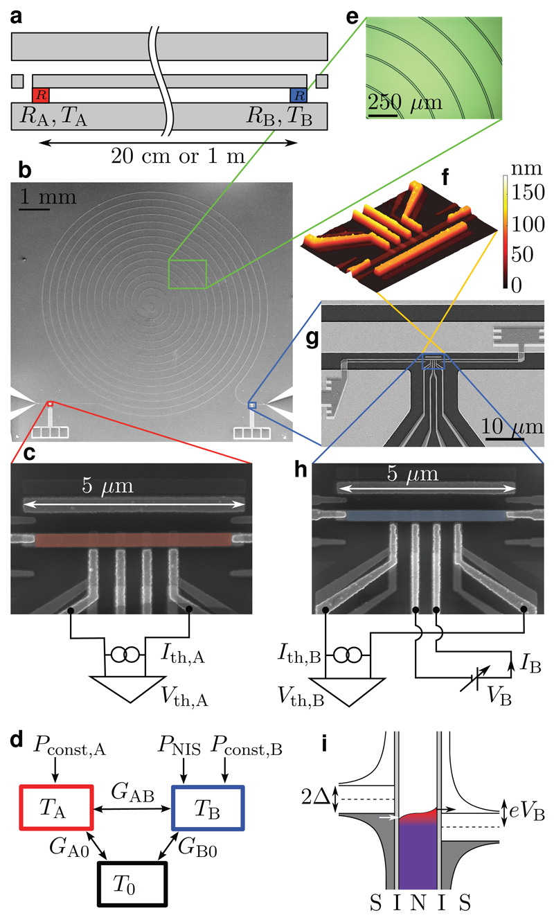
Figure 1. Sample structure and measurement scheme.
a, Schematic illustration of a coplanar transmission line terminated at different ends by resistances RA and RB at electron temperatures TA and TB, respectively. b, Scanning electron microscope (SEM) image of a fabricated transmission line with a double-spiral structure. c, h, False-colour SEM images of the normal-metal islands together with a simplified measurement scheme. e, Optical micrograph of the waveguide. f, Atomic force microscope image of Island B highlighting the thicknesses of the nanostructures. g, SEM image showing how the normal-metal island is connected to the ground plane and to the centre conductor. Micrographs (c, f, g, h) are from Sample A1, and (b, e) are from a similar sample. h, Thermal model indicating the thermal conductance between the Islands A and B, GAB, and those from the islands to the phonon bath at the temperature T0, GA0 and GB0. Constant powers Pconst,A/B and control power PNIS are also indicated by arrows. i, Schematic diagram for cooling of the normal metal due to single-electron tunnelling (arrows) in a pair of NIS junctions biased at voltage . The densities of states in the superconductors (S) are shown by black solid lines whereas the Fermi distribution is indicated in the normal metal (N).

