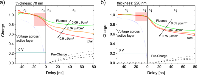
Figure 3. Early time evolution of carrier recombination dynamics in PCDTBT:PCBM devices.
The total extracted charge Qtot (solid colored lines) and pre-charge Qpre (dashed lines) is plotted as a function of delay for different laser fluences including negative delays as described by Fig. 2 for 70 nm (a) and 220 nm (b) active layer thickness. Data have been normalized to yield the same total charge at a delay time of −35 ns. Also shown is the build-up of the electric field across the device as estimated by integrating the capacitive transient in the dark over time (dotted blue line). The situation where short circuit condition (0 V across the active layer) is reached is indicated by a dark green line. Recombination already sets in during the rise of the extraction field for the 70 nm thick sample, but not for a 220 nm active layer thickness. For the thick (thin) device, an active area of 1 mm2 (0.5 mm2) was chosen to closely match the RC-time of both devices. The experimental conditions where the same as in Fig. 1b, with Vpre chosen to be close to the maximum power point at 1 sun illumination.

