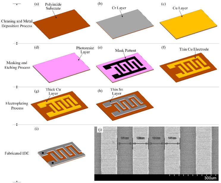
Figure 4.
Preparation procedure of the IDE: (a) polyimide substrate; (b) thin Cr layer on the polyimide substrate; (c) depositing a thin Cu layer on the Cr layer; (d) photoresist layer, (e) transferring the mask pattern onto the photoresist layer; (f) etching the unmasked metal layers; (g) depositing the thick Cu layer onto the thin patterned Cu layer via electroplating; (h) depositing the thin Sn layer onto the thick patterned Cu layer; (i) cutting the residual polyimide substrate; and (j) SEM image of the surface of the interdigitated electrode (IDE).

