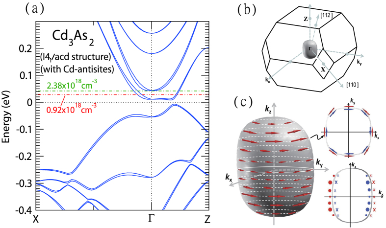
Figure 4.
(a) A calculated band structure of Cd3As2 with I41/acd space group symmetry and Cd antisite defects. The two dotted lines correspond to the Fermi level locations for needle A and B, respectively, determined from the experimental values of Fermi surface area. (b) The calculated 3D Fermi surface with an energy of ≈0.04 eV above the gapped Dirac node close to the Fermi level of our samples suggests a slightly distorted Fermi sphere in Cd3As2. [112] and [200] crystal directions are indicated corresponding to the long-axis directions for needle A and B, respectively. (c) The spin texture over an outer Fermi surface. Red and blue arrows indicate spin texture on the outer and inner Fermi surfaces, respectively, where the size of the arrows indicates the spin polarization. The lower inset shows the spin texture profile on kx − kz plane, while the upper inset is a top view of the Fermi surfaces at finite kz indicated by the black arrows.

