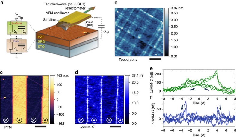
Figure 1. Microwave imaging of conducting domain walls.
(a) Schematic of the sample and sMIM microwave probe on an atomic force microscope (AFM) cantilever. An 100-nm-thick epitaxial thin film of Pb(Zr0.2Ti0.8)O3 (PZT) with a 50-nm-thick SrRuO3 (SRO) bottom electrode is deposited on an SrTiO3(001) (STO) substrate. Microwaves of a frequency f≈3 GHz are delivered to the sensing tip of the probe and to a sample through a stripline fabricated on a silicon nitride AFM cantilever. A reflectometer measures amplitude and phase of the wave reflected from the tip, and represents the results as a change of the admittance Y=G+i2πfC of the tip–sample system through two channels sMIM-G and sMIM-C, corresponding to the conductance G and capacitance C, respectively. Due to the capacitance of the space charge layer or conduction-blocking layers on the surface, electrical behaviour of the film surface can be described by a parallel resistor–capacitor circuit Gs||Cs shown in the lumped elements diagram. The intrinsic dielectric response and conduction of the material bulk are represented by the pair Gb||Cb. Capacitor Ccpl represents the large coupling capacitance between the SRO bottom electrode and the microwave probe shield. (b) Image of the surface topography. (c) Combined out-of-plane PFM image showing a stripe domain structure with polarization P orientated up ⊙ and down ⊗ in the ferroelectric domains as indicated in the image. (d) sMIM-G image (that is, a map of the variation ΔsMIM-G of the reflectometer sMIM-G signal) clearly reveals conductivity in the walls of the stripe domains seen in b. Images in b–d were obtained from the same area of the pristine PZT film. (e) Signal from the sMIM capacitance channel and (f) simultaneous signal from the sMIM conductance channel as functions of d.c. bias applied to the probe at a single point on the pristine film. Arrows indicate direction of the hysteresis. The signal in f is shown in respect to a reference signal approximately corresponding to the domain bulk. The images in b–d were acquired with a zero d.c. bias applied to the probe. Scale bars, 1 μm (b–d).

