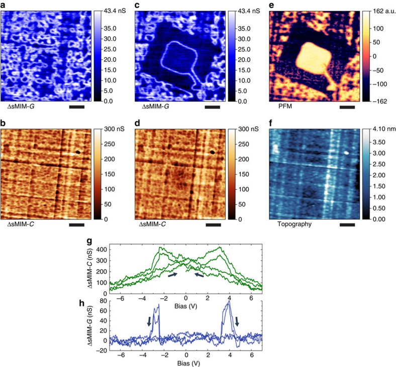
Figure 2. a.c. conductivity and manipulation of conducting domain walls in the annealed PZT film.
Images in a–f were obtained from the same area of the annealed film with a zero d.c. bias of the probe. (a) sMIM-G image, where conducting walls of spontaneous domains of a few-hundred-nm size are clearly seen. (b) sMIM-C image recorded simultaneously with the image in a. (c) sMIM-G image of the box-in-box domain structure written by the probe after the image in a was taken. Spontaneous domains and domain walls were erased inside the structure; the domain walls of the structure are conducting. (d) sMIM-C image recorded simultaneously with the image in c. (e) Combined out-of-plane PFM image acquired right after the image in c. (f) Image of the film surface topography recorded simultaneously with the image in e. Comparing images in b–d with the image in f, it is seen that the sMIM-C signal is dominated by a cross-talk with the surface topography. No traces of domain walls are seen in d. (g) Single-point signal from the sMIM capacitance channel and (h) simultaneous signal from the sMIM conductance channel as functions of d.c. bias applied to the probe for the annealed film. Arrows indicate the direction of the hysteresis. The signal in h is shown in respect to a reference signal approximately corresponding to the domain bulk. Scale bars,1 μm (a–f).

