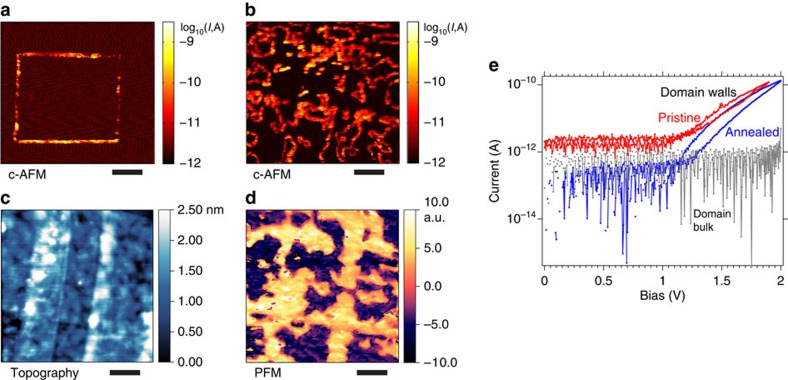
Figure 3. d.c. conduction of domain walls in PZT.
(a,b) Conductive AFM (c-AFM) images of the d.c. current, I, in the PZT film obtained with a metal-coated AFM probe in ultrahigh vacuum. Probe bias in a and b was fixed at +1.9 V. The image in a reveals a conducting domain wall written in the pristine film; the image in b shows a spontaneously formed network of conducting domain walls in the annealed film. (c,d) Image of surface topography and a combined out-of-plane PFM image, respectively, acquired simultaneously from the annealed film. The spots on the film, where images in b–d were recorded are different, but located close to each other. (e) Probe current versus bias for wall locations and for the domain bulk away from walls. Red, blue and grey correspond, respectively, to a domain wall in the pristine film, a domain wall in the annealed film and domain bulk (which does not show detectable conduction at d.c. both in the pristine and annealed films). Scale bars, 280 nm (a); 400 nm (b–d).

