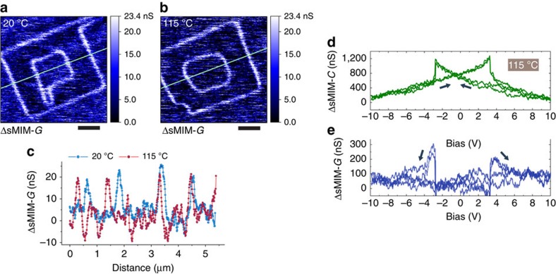
Figure 4. Temperature dependence of the a.c. conduction of domain walls.
(a,b) sMIM-G images of box-in-box domain structures written and imaged at different sample temperatures. The images were acquired with a zero d.c. bias of the probe. The image in a was obtained at room temperature, and the image in b was obtained at a sample temperature of 115 °C. As seen, the intensity of the domain wall response in respect to the background is the same for the images in a and b. This is further illustrated in c. (c) Signal profiles along the green lines in images (a,b). Blue and red correspond to room temperature and 115 °C, respectively. The curves were slightly offset along the vertical axis for the ease of comparison. Note that the geometry of the box-in-box structure is distorted in b due to thermal drift. (d) Single-point signal from the sMIM capacitance channel and (e) simultaneous signal from the sMIM conductance channel at a sample temperature of 115 °C as functions of d.c. bias applied to the probe for the annealed film. Arrows indicate the direction of the hysteresis. The signal in e is shown in respect to a reference signal approximately corresponding to the domain bulk. Signals in d and e are stronger than in other experiments described in the paper because of an increased sample–probe force and, consequently, a larger sample–probe contact area. This was done to increase signal-to-noise ratio to compensate for the increase of the noise level associated with the elevated temperature of the probe. Scale bars, 1 μm (a,b).

