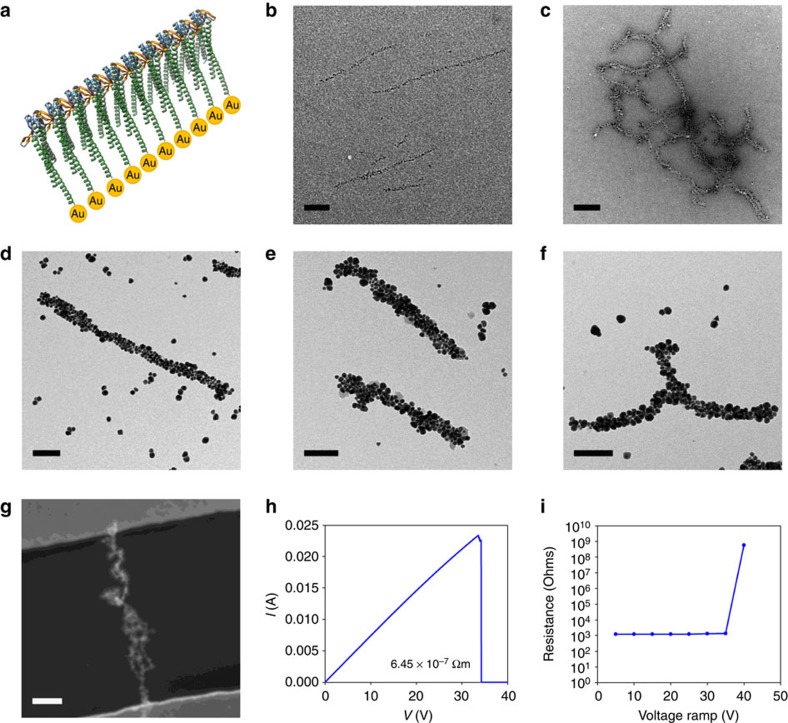
Figure 4. The controlled positioning of nanoparticles on filament templates.
(a) Schematic diagram of gold nanoparticles attached to the C terminus of γPFD subunits (scale bar, 200 nm). (b) TEM image of 1.8-nm and, (c), 5-nm Ni-NTA-nanogold arrayed onto filaments of γPFD. (d) TEM image of continuous Au nanowires created by deposition of additional gold on filaments with arrayed Ni-NTA nanogold. (e) TEM image of TERM-(E-coil) nanowires filaments capped at a 1:50 ratio to produce uniform lengths. (f) Conductive nanoarchitecture were created by assembling TERM-(E-coil) capped filaments with a three-way connector and patterned with gold. Scale bars, (c–f) 100 nm. (g) Scanning electron microscopy image of a filament nanowire that bridges the gap between electrodes (scale bar, 500 nm). (h) Two-terminal current-voltage I-V plot of a γPFD-Au nanowire. (i) Resistance versus voltage ramp plot.

