Fig. 2.
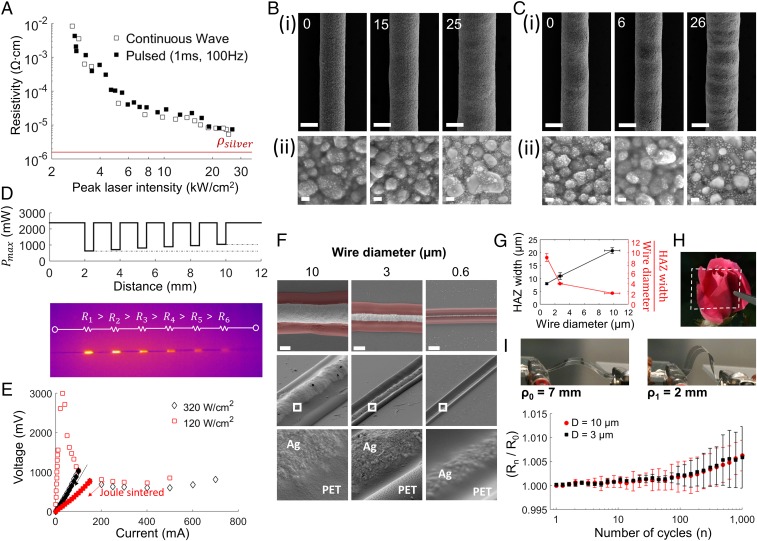
Electrical conductivity and nanostructure of laser-annealed silver wires. (A) Silver resistivity decreases with increasing laser intensity. The red line represents the resistivity of bulk silver metal. Microstructure of silver wires annealed by (B) CW and (C) pulsed (1-ms, 100-Hz) laser illumination. Numbers indicate peak illumination intensity in kW/cm2. [Scale bars, 10 µm (C, i), 100 nm (C, ii).] (D) A varying laser intensity profile (Top) results in corresponding IR emissions from resistive elements as current is passed through the wire. Each resistor is ∼500 µm in length. (E) I-V characteristics of two resistors formed at different laser intensities. Current is stepped up (unfilled) to a certain level, and then stepped down (filled). (F) SEM images of various diameter wires laser annealed onto PET films. (Top Row) Top view, false colored to reveal the HAZ extending from the printed silver wires. (Scale bar, 5 µm.) (Middle Row) Oblique views of printed silver wires. (Bottom Row) Magnified images of the interface between the printed silver (Ag) wire and PET substrate. (G) The width of the HAZ (black line) and the ratio of the HAZ width and the silver wire width (red line) vary with the diameter of the printed and annealed wires. Five wires are tested for each diameter. (H) An array of silver wires, with submicrometer widths, is printed onto a transparent PET film across a 1-cm2 area, using a wire spacing distance of 500 µm. The resulting film, indicated by the white dashed line, remains transparent. (I) Cyclic testing of the electrical resistance of 3- and 10-µm silver wires printed onto a 20-µm-thick PET film. The radius of curvature alternates between 2 and 7 mm. The graph shows the variation of resistance after n cycles (Rn) normalized to the initial resistance before cyclic testing (R0). Three wires are tested for each condition.

