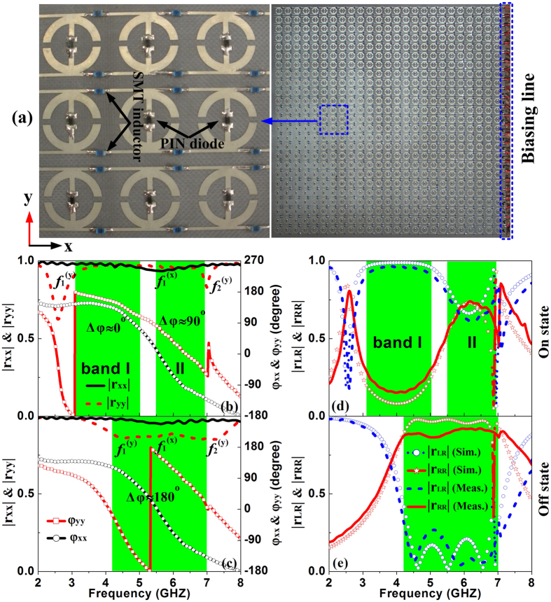
Figure 5. Picture and the measured LP and CP reflection coefficients of the fabricated TMS.
(a) The building block of the TMS are connected by the SMT inductors along x –direction with the biasing line to control the voltage of PIN diode. (b,c) In LP basis, the reflection phase difference between φyy and φxx is kept at about 0o in Band I (3.11~5.01GHz) and about 90° in Band II (5.51~6.94 GHz) in the “On” state and is kept at about 180° in an ultra-wide band (4.21~7.01 GHz) in “Off” state. (d,e) In CP basis, the TMS functions as a CP helicity convertor in Band I and CP helicity hybridizer (i.e., CP polarizer) in Band II in the “On” state, and the CP helicity keeper in the ultra-wide band (4.21~7.01 GHz).

