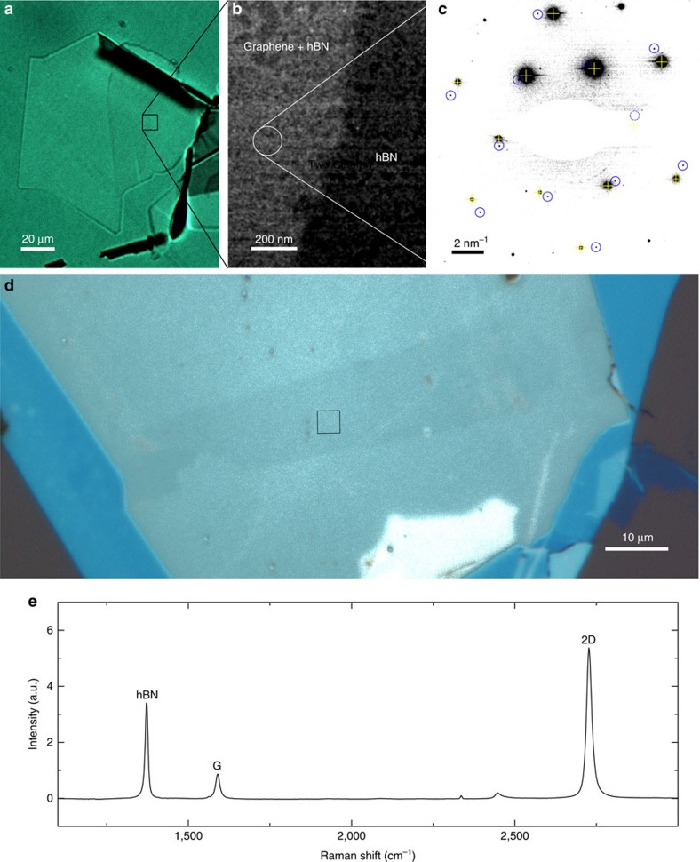
Figure 4. TEM and Raman spectroscopy.
(a) Optical transmission image of a graphene flake adhered to hBN on PPC/PDMS. (b) Dark-field tilted beam TEM image of region indicated in a. A discontinuous layer of amorphous carbon is visible. The objective aperture has been positioned to provide lighter contrast from the graphene region. (c) Selected area electron diffraction pattern from region indicated in b. The contrast has been enhanced to show both the monolayer graphene diffraction pattern (reflections indicated with blue circles) alongside the hBN diffraction pattern (indicated with yellow crosshairs). Points masked by the beam stop or by nearby stronger reflections are indicated with dashed versions of the same. (d) Enhanced contrast optical image of the encapsulated graphene. The boxed region indicates the region where the spectrum in e was acquired. Maps of the I(2D)/I(G) ratio and G peak full width at half maximum (FWHM) are available in Supplementary Fig. 6. (e) Raman spectrum of hBN-encapsulated graphene fabricated by the hot pick-up method, normalized to the G peak intensity. The I(2D)/I(G) peak ratio is 5.8 (with Lorentzian fits to the peaks (R2>0.994) indicating a ratio of 6.12±0.02), with a FWHM of 14.2±0.5 cm−1.

