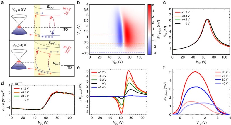
Figure 2. Enhancement of photoresponse using a top-electrode.
(a) Energy level diagrams of the graphene–CQDs interface without (top) and with (bottom) positive VTD voltage applied. Positive VTD voltage induces electrical field perpendicular to the graphene–CQDs interface and increases the depletion width and charge collection efficiency. The yellow area qualitatively indicates the change of depletion width on the scale below it. (b) Colour map of the photovoltage response as a function VBD and VTD for 100 mW m−2 illumination with a 635-nm light. Positive (red) and negative (blue) area correspond to injection of photo-generated holes into the n- and p-doped graphene. Dashed lines indicate the positions of cross-sections (e). (c) Resistance of the device's active area as a function of VBD for fixed values of VTD specified in the legend. (d) Transconductance of the device as of VBD for fixed values of VTD specified in the legend. Presented curves demonstrate no significant change with increasing VTD. (e,f) Photovoltage response, in absolute values, taken from cross-sections of the colour map (b) at fixed values of VTD (e) and VBD (f) as specified in the legends.

