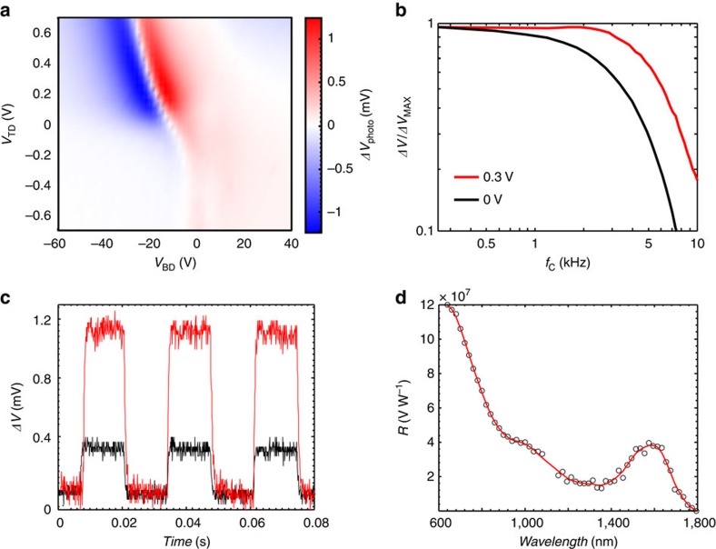
Figure 5. Visible/SWIR phototransistor characteristics.
(a) Colour map of photovoltage response for a hybrid photodetector with large PbS CQDs as a function of the VBD and VTD. Positive (red) and negative (blue) area correspond to injection of photo-generated holes into the n- and p-doped graphene. The optimal VTD of 0.3 V results in a threefold increase of the photoresponse amplitude. Illumination is with 635-nm light and irradiance of 0.1 W m−2. (b) Photoresponse of the device as a function of the optical modulation. (c) Temporal response traces of the device at VTD=0 V (black) and VTD=0.3 V (red), demonstrating stable sub-millisecond photoresponse. (d) Spectral responsivity of the device with large PbS CQDs with exciton peak at 1,600 nm. The spectral sensitivity is determined by the absorption spectra of the quantum dots that can be readily tuned at their synthesis. The red line is a guide to the eye.

