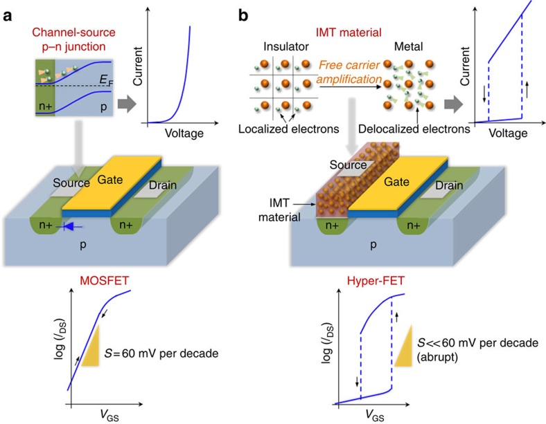
Figure 1. Schematic device design of hyper-FET and working principle.
(a) Conventional MOSFET and its transfer characteristics (channel current IDS versus gate bias VGS) for a fixed drain-to-source voltage VDS. The channel-source p–n junction, modulated by the gate terminal, controls the injection of carriers into the channel limiting the switching slope (S) of the MOSFET to 60 mV per decade (Boltzmann limit). (b) Proposed hyper-FET in which an insulator-to-metal transition (IMT) material that shows electrically induced abrupt resistivity switching is electrically integrated in series with the source of a conventional MOSFET. For a given VDS, the gate-terminal voltage VGS modifies the current flowing through the MOSFET and the IMT material in series, triggering an abrupt phase transition. The associated delocalization of localized carriers (free-carrier amplification) across the IMT results in an abrupt decrease in the resistance of the source, enhancing the switching slope characteristics beyond the intrinsic limits of a conventional p–n junction.

