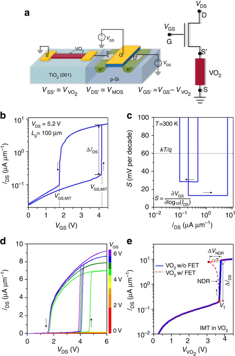
Figure 2. Experimental demonstration of a VO2-based hyper-FET.
(a) Schematic of a hyper-FET consisting of a two-terminal VO2 device ( =4 μm;
  =2 μm) in series with the channel of a conventional Si n-MOSFET (Lg=100 μm; W=100 μm). VVO2 is the voltage across the VO2 device and VGS′ is the effective gate-to-source voltage across the MOSFET. (b) IDS–VGS transfer characteristics of the hyper-FET exhibiting abrupt and reversible modulation of the channel current IDS as a function of the gate-source voltage VGS. The abrupt turn-ON and turn-OFF of the hyper-FET corresponds to the IMT and MIT in VO2, respectively. (c) Switching slope (S) as a function of IDS revealing the steep-slope characteristics (S<60 mV per decade) of the hyper-FET during the forward and reverse gate bias sweep. (d) Output characteristics (IDS–VDS) of the hyper-FET with excellent current saturation. (e) Current versus voltage characteristics of the VO2 device with (red) and without (blue) the MOSFET in series, illustrating the electrically triggered abrupt IMT. The channel resistance of the MOSFET acts as a series resistor, modifying the current–voltage dynamics through a feedback and inducing a negative differential resistance NDR (red) across the phase transition in VO2. The NDR reduces the voltage across the VO2 by ΔVNDR. The current has been normalized to the width of the Si n-MOSFET to show that the abrupt IMT in VO2 triggers the abrupt turn-ON of the hyper-FET shown in b.

