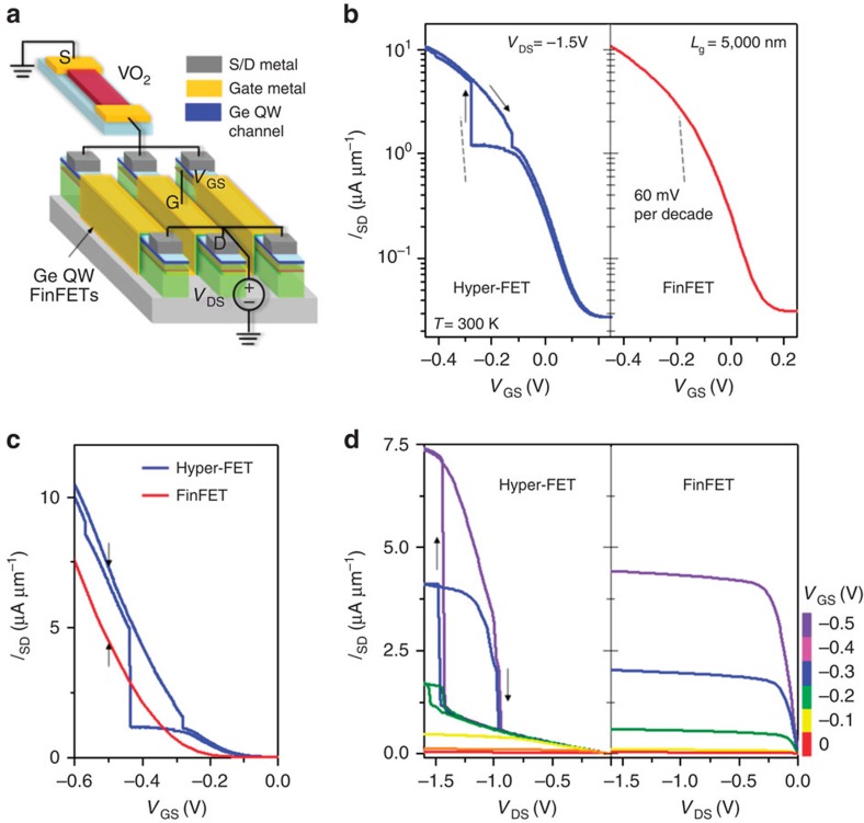
Figure 4. Experimental demonstration of a low-voltage p-type hyper-FET.
(a) Schematic of the p-hyper-FET consisting of a series combination of scaled VO2 ( =200 nm) and multi-channel (=200 fins) p-type Ge quantum-well FinFET (Lg=5,000 nm). (b) Transfer characteristics (ISD–VGS) of the hyper-FET and the FinFET (stand-alone). (c) The p-hyper-FET shows a ∼60 % higher ON-state current (ISD,ON) in comparison to the stand-alone FinFET over a gate-voltage window of −0.5 V at matched OFF-state current. (d) Output characteristics (ISD–VDS) of the p-hyper-FET and the conventional FinFET.

