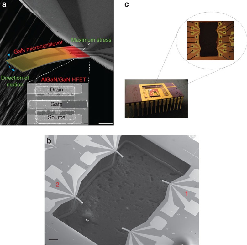
Figure 1. Images of AlGaN/GaN HFET-embedded GaN microcantilevers.
(a) SEM image of GaN microcantilever with AlGaN/GaN HFET embedded at the base (scale bar, 50 μm). The inset shows a magnified section containing the HFET (scale bar, 2 μm). The microcantilever is coded with false colour along its length to show the stress distribution when it is deflected. (b) SEM image of a representative chip with four microcantilevers overhanging in a rectangular trench (scale bar, 500 μm). The microcantilevers investigated in this study are as marked 1 and 2. (c) Picture of a 28 pin DIP package with the microcantilever chip wire bonded. The inset shows a close-up of the wires bonded to the bias pads.

