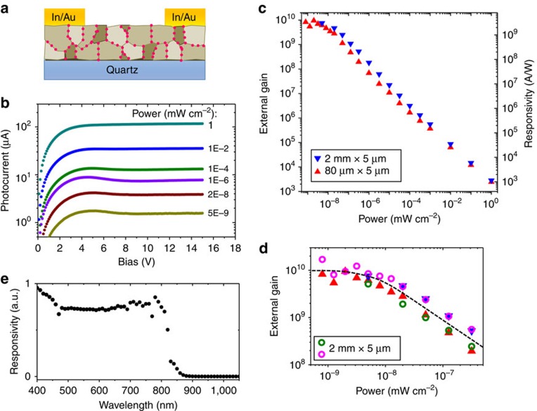
Figure 4. Photoconduction.
(a) Schematic of the photoconductor device structure. (b) Photocurrent versus bias of a representative photoconductor, measured with 500 nm monochromic light over a range of incident power (as labelled in the figure). Channel thickness: 320 nm; length: 5 μm; width: 2 mm. Extended data on current, photocurrent and dark current is presented in Supplementary Fig. 7. (c) External photoconductive gain and responsivity of photoconductor devices. Incident wavelength: 500 nm. Bias: 10 V. Channel width and length are labelled in the figure, where the inverted triangle points represent the same device as that in b. (d) External gain of four devices at small photon power, where the triangle and inverted triangle points are the same as that in c. The dashed line is drawn to guide the eye. (e) Spectral response of a 2 mm × 5 μm device. The fluctuations are not due to the noise in the detector, but rather the spectral intensity variations of the light source (Supplementary Fig. 8).

