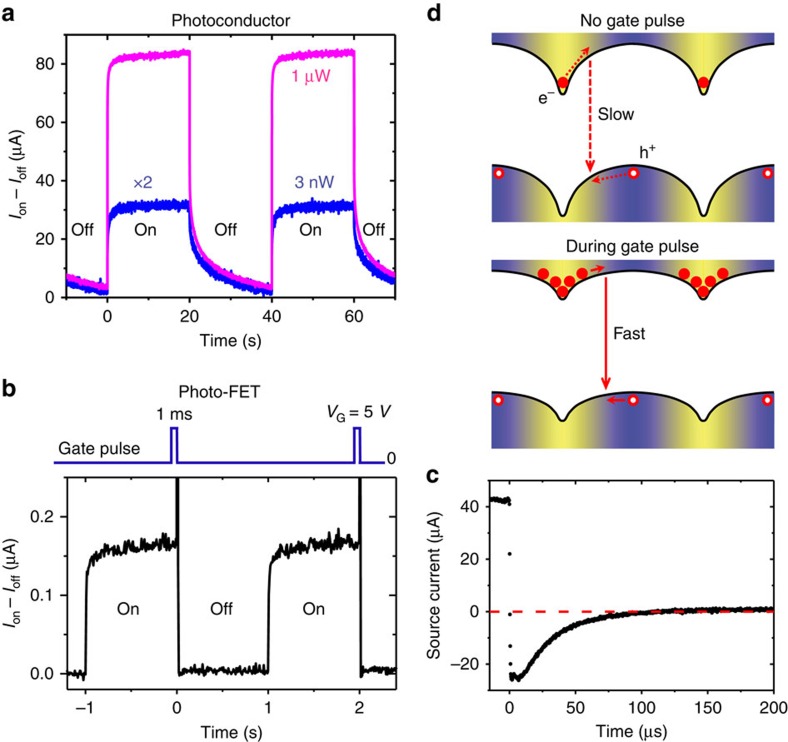
Figure 6. Temporal response.
(a) Time trace of the photocurrent in a photoconductor, with the on/off modulation (interval: 20 s) of 660 nm light with two different intensities, 1 μW and 3 nW (over the channel region). Note that the photocurrent at 3 nW light is amplified by a factor of 2. Channel geometry: 2 mm (width) × 5 μm (length) × 320 nm (thickness). Bias: 1 V. (b) Temporal response of photocurrent in a photo-FET, in the presence of a 1 ms gate pulse synchronized with the on-to-off switch of the 660 nm light at 0.4 μW (on/off modulation interval: 1 s). Channel geometry: 3 mm (width) × 40 μm (length) × 70 nm (thickness). VD=1 V. (c) Transient photocurrent response (within 200 μs) of the same photo-FET device as in b. Note that the source current shown in c is the total current flowing into the source, with no dark current subtraction, while Ion–Ioff in a and b represents the on-state current minus the dark current. (d) Schematic of the band bending and carrier recombination with or without the gate pulse reset.

