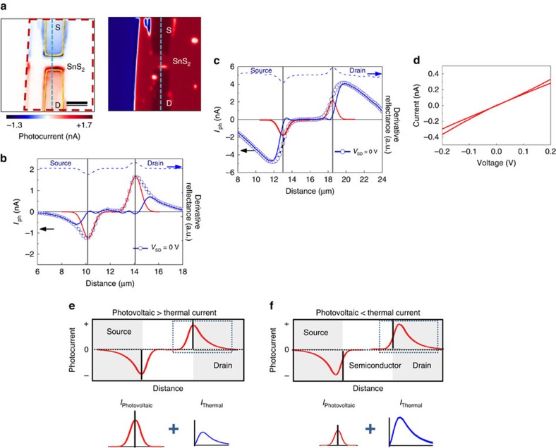
Figure 3. Photocurrent composition measurement and analysis for two SnS2 samples of thickness.
(a) Photocurrent map (left) and reflection image (right). Scale bar, 3 μm. (b) Photocurrent profile at 0 V source bias with laser wavelength of 405 nm (3.06 eV) and power of 195 μW for 100 nm thickness, which shows photovoltaic current-dominated Gaussian profile. The derivative of reflectance along the blue dashed line shown in the reflectance measurements (right of a) plotted in the photocurrent profile. (c) Photo-TE current profile from along the blue dashed line in Fig. 2b, which demonstrates a thermocurrent-dominated profile. (d) I–V curve of the Pt/Ti/SnS2 contact, demonstrating that a good ohmic contact is formed on the SnS2 material. (e,f) Expected current profile and decomposition of contributing components for the 100- (e) and 16-nm (f) samples. Shaded areas indicate S/D electrode regions. The measured photocurrent in the dotted blue rectangles of e (top) and f (top) are decomposed into their respective Gaussian photovoltaic (bottom left) and thermal (bottom right) components; their sum results in the profile shown in each respective dotted blue rectangle region.

