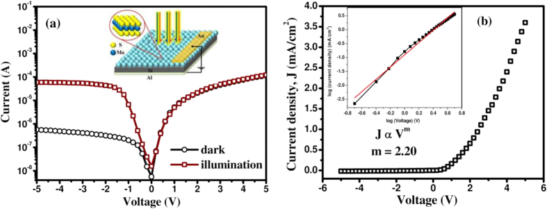
Figure 5.
(a) Current-voltage characteristics of fabricated heterojunction, using ~2 nm MoS2 quantum dots on Si, under dark and illumination condition. The inset shows the schematic structure of the heterojunction device. (b) J–V characteristics of fabricated p-n heterojunctions under dark condition, at room temperature. The inset shows the logarithmic J–V curve for the heterojunction fitted with a power law J ∝Vm corresponding to the trap-charge-limited current transport.

