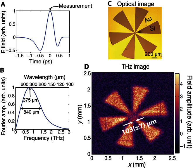
Fig. 2. Pulsed THz imaging.

(A) Electric field of our THz pulse recorded in the time domain using electro-optic sampling. The arrow shows the measurement point, at the peak of the THz field, for which images are recorded. (B) Normalized Fourier transform of our THz pulse. The central wavelength is approximately 375 μm, with a full width at half maximum of 840 μm. (C) Optical image of a resolution test target. Au marks the regions spanned by the gold film, whereas the regions that are marked “Si” show the exposed silicon wafer. (D) Image (128 × 128 THz) of the resolution test target in (C) obtained via a full set of Hadamard masks. The pixels are 20 μm in size. The arrows indicate the imaging resolution, evaluated as the maximal distance between the arms of the cartwheel for which the image contrast is diminished due to diffraction.
