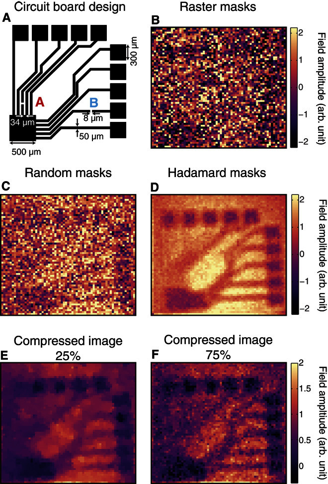
Fig. 3. Hadamard versus random versus raster imaging.

(A) Circuit board design, where black indicates conducting, metallic regions. The individual wires are 50 μm in width, and 8-μm breaks have been introduced at points marked by the letters A and B. (B) Image acquired using raster scanning of a single opaque pixel. (C and D) Comparison of the same image acquired with a full set of masks derived from random and Hadamard matrices, respectively. (E and F) Compressed images obtained via random masks, where the number of measurements is 25% (E) and 75% (F) of the total number of pixels (we use a total variation minimization image recovery algorithm; see section S6 for more details). In all images, the THz electric field is polarized horizontally, and the number of pixels is 64 × 64 with 40-μm pixels. The signal acquisition time for a single measurement is 500 ms. Because of the considerably larger noise in the measurement, we have scaled the image in (B) by 0.25 to use the same color scale as in (C) and (D).
