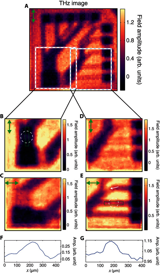
Fig. 4. Imaged polarization effects.

(A) Images (64 × 64) of circuit board in Fig. 3A with vertical polarization. Pixels are 40 μm. We see that the contrast of each of the individual wires in the circuit depends on the THz polarization, with the highest contrast seen for polarization parallel to the wires. (B to E) Images (64 × 64) of the square regions in (A). Polarization is shown by the green arrow on the top left corner of each picture. Pixel size is 20 μm, and images have been denoised using the algorithm described in section S7. We see that the very subwavelength wiring breaks [marked by circles in (B) and (E)] give rise to transmissive regions in the THz image when the THz polarization is parallel to the wire. In (E), the diagonally orientated wire (indicated by the white arrow) also shows low contrast. Every image has been obtained via a full set of Hadamard masks. (F and G) Line plots through the 8-μm gaps in (B) and (E) with amplitude and space on the vertical and horizontal axis, respectively. The spatial coordinates of the plots are indicated by green rectangles in (B) and (E).
