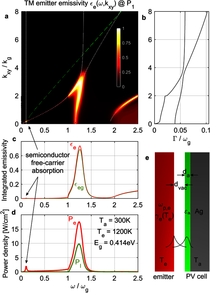
Figure 1. Results for optimized structure of Fig. 1e, at Te = 1200 °K, Ta = 300 °K and with Eg = 4kBTe = 0.414 eV.
(a) TM emitter emissivity  (color plot) and dispersion of system modes (dotted white lines); dashed green line is the semiconductor-material radiation cone. (b) Loss rates of the two system modes. Note the ‘kink’ in one mode loss-rate due to the onset of semiconductor inter-band absorption. (c) TM emitter emissivity
  (red line) and emitter-bandgap transmissivity
  (green line) integrated over kxy. (d) TM emitter power Pe(ω) (red line) and load power Pl(ω) (green line) densities at the optimal-efficiency load voltage. (e) Proposed TPV structure of a plasmonic emitter and a silver-backed semiconductor thin-film absorber. The semiconductor εa includes free carriers to model the front electrode. The coupled emitter-SPP and absorber-waveguide modal energy profiles are shown qualitatively.

