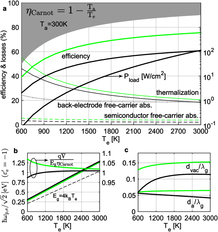
Figure 2. Optimization results vs emitter temperature Te.
Ag back-electrode (black lines), PEC back-electrode (green lines). (a) Left axis: Efficiency (thick solid lines), thermalization losses (thin solid lines), semiconductor free-carrier absorption losses (dashed lines) and Ag back-electrode losses (dotted line); grey region is the Carnot limit on efficiency. Right axis: Output load power density. (b) Left axis: Optimal emitter plasma-frequency (scaled to cutoff frequency of a SPP on interface with vacuum, to be compared with Table 1); dashed black line shows Eg = 4 kBTe, for guidance. Right axis: Optimal load voltage (normalized to Eg and the Carnot efficiency). (c) Optimal vacuum-gap width and semiconductor thin-film thickness (normalized to λg).

