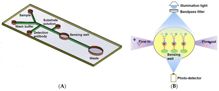
Figure 1.
Schematic of the Microfluidic ELISA chip layout (not to scale) (A) and Principle of the on-chip absorption detection with the miniaturized optical sensor device (B). The diameters of the sensing and waste wells are 2.5 mm and 6 mm, respectively. The width of the main channel and the branch channels are 200 μm and 100 μm, respectively. All other wells are 0.75 mm in diameter to fit the loading syringe tip.

