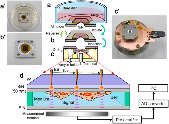
Figure 1. Experimental set-up and dielectric microscopy using a culture dish holder and SE-ADM system.
(a,a’) Al holder with W-coated SiN film is attached in the bottom of a medium-filled culture dish. After 4–5 days of culture, cells in the holder formed a confluent monolayer on the 50-nm-thick SiN film. (b,b’) The holder containing cultured cells was separated from the plastic culture dish after removing part of the medium. (c,c’) The Al holder was attached upside down onto another SiN film on a square acrylic plate. These components were sealed with an O-ring and four screws. The sample holder with cells in the medium was mounted on the pre-amplifier attached to the sample stage. (d) Schematic figure of our high-contrast imaging method with low-level radiation damage to untreated cells in the medium under W-coated SiN film. EB irradiation of the W-coated SiN film causes electron scattering and absorption in the film, and negative potential in EB-irradiated position. This negative electric potential is transmitted to the bottom SiN film through the cultured cells in the medium.

