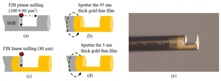
Figure 7.
The schematic diagram of key procedures. (a) The micro-cavity is machined by FIB. (b) A 95 nm thick gold thin film is sputtered. (c) The gold film on the left of the micro-cavity is removed by FIB milling. (d) A 5 nm thick gold thin film is sputtered. (e) Image of the fabricated sensor head.

