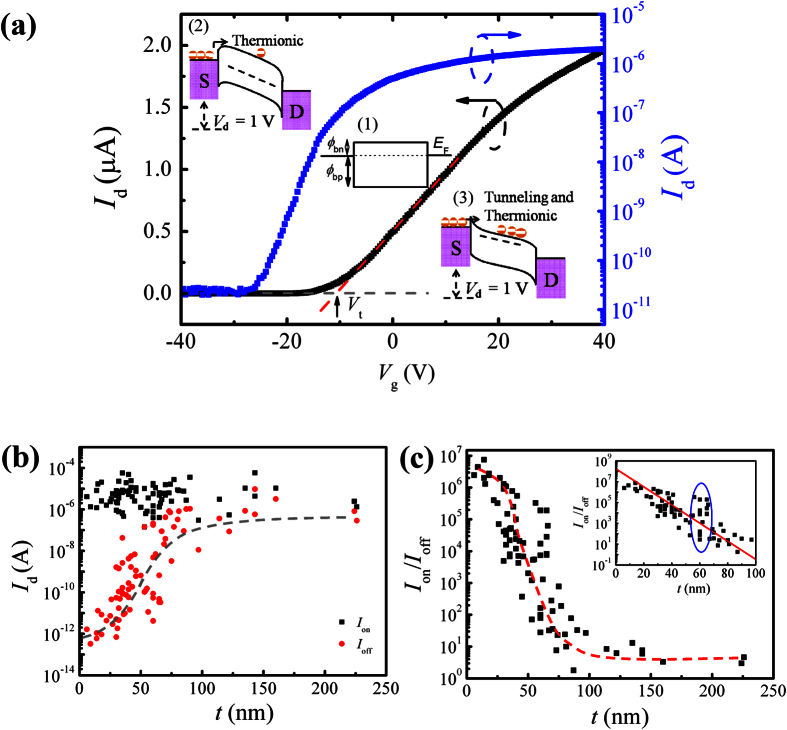
Figure 3.
(a) Transfer characteristics of a representative transistor with a 30-nm-thick MoS2 film on a linear scale (left y-axis) and a log scale (right y-axis). The threshold voltage, Vt, is determined by the intercept on the x-axis with the regression fitted line to the linear scale characteristics. The insets represent the energy band diagrams corresponding to the applied Vg in three distinct regions: (1) at flat band, (2) below threshold, and (3) above threshold. ϕbn and ϕbp indicate electron and hole SBH, respectively. (b) Dependence of Ion and Ioff on MoS2 flake thickness. The grey dashed line serves as a guide to the eye. (c) Thickness-dependence of Ion/Ioff. The red dashed line serves as a guide to the eye. Inset is the zoom in for the first 100 nm. The red solid line in the inset is a linear fit on the semi-log scale.

