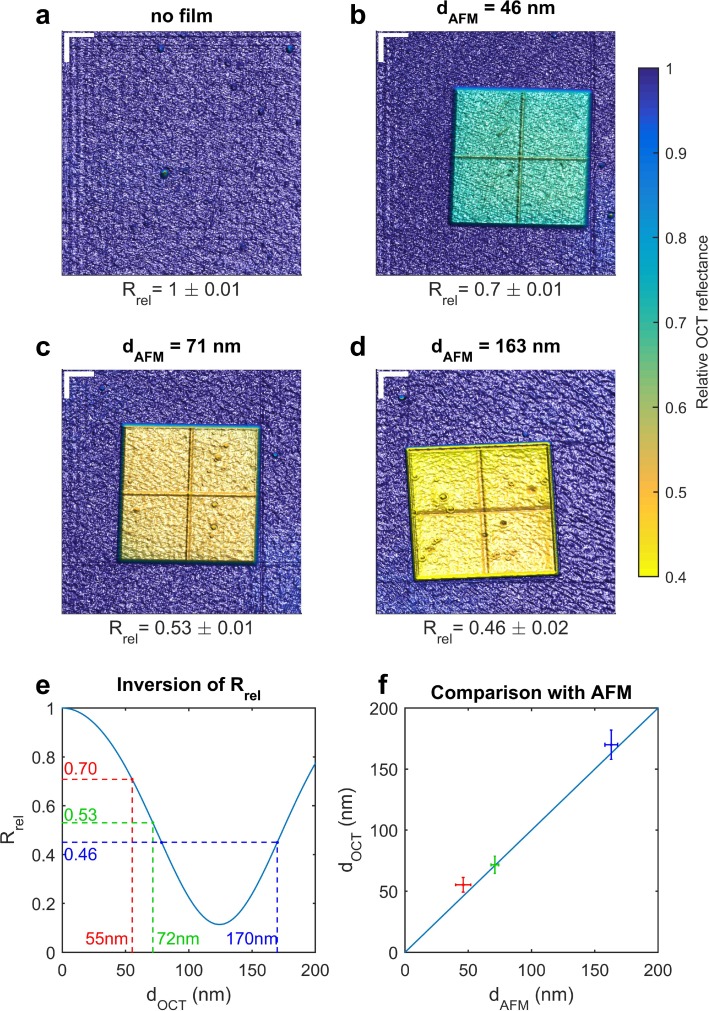
Fig. 4.
(a–d) En face OCT reflectance maps of fabricated samples: (a) silicon substrate only, (b–d) island of SU-8 photoresist film (1 mm × 1 mm) deposited on silicon substrate. Film thicknesses are (b) 46 ± 6 nm (b) 71 ± 2 nm (c) 163 ± 5 nm, as measured with the AFM (mean ± roughness). Comparing the maps (b–d), differences in the OCT reflectance can clearly be observed. (e) Inversion of Rrel to obtain the OCT thickness value. (f) Comparison between the AFM and OCT thicknesses values. Error bars correspond to OCT thickness uncertainty (vertically) and to AFM roughness (horizontally). Lateral scale bar (top-left corner in Fig. 4(a–d)) corresponds to 225 μm. The color scale is the same for each sample. The cross seen on the islands is an artifact of the fabrication process.

