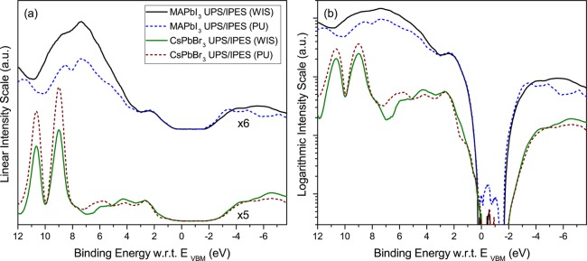
Figure 4.
Comparison between UPS and IPES spectra taken from MAPbI3 (top) and CsPbBr3 (bottom) samples grown at WIS and PU. The PU films, grown on ITO, were 400–500 nm thick. Spectra are referenced to the VBM, EVBM = 0 eV, and plotted on (a) a linear scale and (b) a logarithmic scale. The difference between the band gap energies of the two compounds (1.6 vs 2.3 eV) is clearly visible in panel b.

