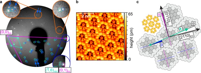
Figure 1.
(a) Room temperature LEED image (incident electron energy 38.0 eV, sample tilted by 15°, logarithmic contrast) of one HBC monolayer on epitaxial graphene (EG), corrected for imaging38 and tilt distortions.39 Dark blue zoom: the (1̅,6) HBC spot (turquoise) and its equivalents do not coincide with first order substrate spots (magenta), rendering the structure not commensurate. EG reconstruction spots (magenta as well) and multiple scattering between HBC and EG (blue) are needed to explain all spots (cf. orange zooms). The blue arrows mark the most intense multiple scattering spots in the simulated lattice and equivalent experimental locations in the upper half of the image. (b) STM image of a mirrored domain at 4.4 K with a sample bias of −3 V and a set point of 3 pA, corrected only for plane tilt. Predominantly, the HOMO is detected (cf. HOMO electron density via DFT in panel c). (c) Orientations from the STM and LEED measurements, where α = θ + β, with θ defined as the unit cell rotation.

